Trying to pass SPI signals through transistors, but it doesn't seem to work

alexandros

Well-known member
I'm trying to build a modular system where modules that contain shift registers can connect to a bus board. To avoid hard-coding the number and positions of these modules on the bus board (there are sixteen sockets where modules can connect, through IDC connectors), I'm trying to detect them, and route the MISO and MOSI signals accordingly.
For example, if a module is connected to a socket, the MISO and MOSI signals will be routed to the respective IDC so they arrive at the module. The serial output of the module will go back to the IDC and further onto the bus board. If no module is connected to a socket, the socket is bypassed, and the MISO and MOSI signals are routed further down the bus board, to the next socket.
To do this, I'm using transistors that determine where the MISO and MOSI signals should go, for every socket. In the first 12 positions or so, this seems to be working fine, but close to the last positions, there is a lot of noise coming in. The traces on the bus board are 0.25mm wide, and the sockets are placed at 25mm from one another.
Could it be that the latch and clock signals are causing this, due to long distances? Is it OK to pass MISO and MOSI signals through several transistors?
I don't care to have a high speed with SPI, so I've tried slowing it down, but it doesn't help. Any tips on why this is not working and how I should solve this problem?
My goal is to build a plug-and-play bus board with generic code that should be loaded once to the Teensy.

Cheers
 
Instead of a tree-like structure, where the signals pass through several transistors, you should consider a bus like structure.

I prefer to use unidirectional voltage level translators like TI TXU0304 for SPI, TXU0204 for UART with hardware RTS/CTS, and TXU0202 for UART RX/TX; with the OE (Output Enable) pin asserted only when that connector is active. All data signals are connected to the translators. When not enabled, the outputs are tri-stated, and won't affect the other signals.

This way, each connector will also need to supply their preferred voltage level from 1.1V to 5.5V. This provides some protection against goofing, especially if you add low forward voltage drop diodes to the outer Vcc (connector side of the voltage translator), and optionally current-limiting (and coupled noise reducing) resistors on the outer inputs.

The only downside is that the TI TXU0n0m translators are not as cheap as a transistor per output connector signal pin (0.78€ to 0.96€ apiece in singles at Mouser). On the plus side, an euro per connector is not that much, they support very high signal frequencies, and handle voltage level translation for you, with a very simple logic level output enable pin (with either logic level).

If you need direction control, then 74LVC1T45 (in SOT23-6), 74LVC2T45, and 74LVC8T245 have a direction pin instead of a output enable pin. You can use a transistor on the microcontroller side VCC pin as an output enable on these, as the outputs are tristated whenever either VCC is low.

All that said, I do often tell everyone playing with Teensies and microcontrollers to keep these unidirectional TXU0n0m voltage level translators for UART, SPI, and generic unidirectional I/O, in stock, because they have saved my butt so often. (SN74LVC1T45 in SOT23-6 can even be dead-bugged, soldered in free air directly to leads to handle a single I/O line.)
The TXU0n0m translators work best if you do add a 0.1µF = 100nF ceramic capacitor (0806, 0603) between each VCC and ground; see e.g. my TXU0202 and TXU0304 DIP adapter boards (public domain). From these, it is also easy to upgrade to full digital isolators like ISO6721 for UART RX+TX or TI ISO6741, which not only handle voltage level translation (1.8V, or 2.25V to 5.5V), but also completely electrically isolate the signals, voltages, and grounds, for maximum safety.
 
I prefer to use Analog Devices ADUM1201 - See Below:
Adum1201-1.png
 
Yep; there are many digital isolator chips available with different configurations (both unidirectional and bidirectional, different number of channels, different channel direction configurations for unidirectional one) that can also do voltage level shifting.

I personally prefer ISO6721 (or ISO6741) over ADuM1201, simply because they fit my needs better with much lower price – ISO6721BDR (1:1) is just 1.72€ in singles in SOIC-8 footprint at Mouser; ISO7741DBQR (3:1) is 2.21€, and ISO7742DBQR (2:2) is 2.22€ in singles in SSOP-16 footprint.
There are technical differences (capacitive coupling versus magnetic coupling in particular) that a hobbyist like me does not need to worry about, but might be important for others. Note that there are different variants of each IC, depending on whether the outputs are high or low when the corresponding input is floating. Floating low is useful for UART TX and RX, for example, because they both are normally high when idle: a disconnected UART looks then the same as a connected UART not sending or receiving data, and no special action is needed to detect UART connects/disconnects.

I do like ADuM3160 and ADuM3166 for USB isolation, and Skyworks Si83xx 6- and 8-channel digital isolators for buses and GPIO. The SI838x, for example, are very nice if you want to interface to 24V logic as used on programmable logic in industrial systems (say, DIY used industrial CNC machine conversion).

The unidirectional UART/SPI/GPIn/GPOut isolators and voltage level shifters do typically want a ceramic 0.1µF = 100nF supply bypass capacitor between each VCC and GND close to the IC, but they are very simple to use.


If the connector will supply power to the module, with no module ever externally powered, there is no need to use isolators. If the module logic levels are also fixed (at say 3.3V, the module having their own voltage level translators if needed), then there is no need for a voltage level translators either; tri-state buffers like 74VHC125, SN74HCS125, 74HC241, 74HC244, etc. would suffice. Some tolerate 5V inputs even when running at 3.3V logic levels; and some have Schmitt trigger inputs, which help with noise rejection.

Tri-state buffers have a (possibly inverted) output enable pin for each signal, or a group of signals. When disabled, the output is tri-stated, high impedance; as if the wire was disconnected. Typically, you'll still need a supply bypass capacitor between VCC and GND near each IC, and a weak (high resistance) pull-up or pull-down resistor on each signal, to ensure all inputs (including unused inputs!) are always high or low, never floating. For a bus scheme, this would mean one shared pull-up/pull-down on each input to the microcontroller (output from a module), and some thought on the use of each I/O line: in particular, having a signal be an output from one module but an unrelated input to another module, can lead to difficulties.
 
For pure shift registers:

Let's assume we use three signals: SCLK, MOSI, and MISO.

Each socket receives SCLK_PREV, MOSI_PREV, and MISO_PREV from the previous socket, forwarding them to the next socket as SCLK_NEXT, MOSI_NEXT, MISO_NEXT. (That is, SCLK_NEXT in socket 2 is the same as SCLK_PREV in socket 3.)

On each socket, signals from the previous socket are connected to SCLK_PREV, MOSI_PREV, and MISO_PREV. The corresponding shift register outputs are SCLK_OUT, MOSI_OUT, and MISO_OUT. Note that we do want to route clock the same way we route the two data signals, to ensure they stay in sync. Although eight pins on the socket connector will suffice (VCC/3.3V, GND, SCLK_PREV, SCLK_OUT, MOSI_PREV, MOSI_OUT, MISO_NEXT, MISO_OUT), I suggest adding an additional PRESENT pin, which is connected to VCC on the module whenever the module is enabled. (That is, you can use e.g. an ON-OFF toggle switch to select whether the module is enabled or not.)

When the module is present, we want SCLK_PREV to be connected/shorted to SCLK_NEXT, MOSI_PREV to MOSI_NEXT, and MISO_NEX to MISO_PREV, with minimal resistance (impedance) and capacitance possible. When the module is not present, we want those to be separate.


The simplest solution is to use a "jumper module" for unused sockets, which simply connects SCLK_PREV to SCLK_OUT, MOSI_PREV to MOSI_OUT, and MISO_OUT to MISO_NEXT, and leaves VCC and GND unconnected. (You do not need the PRESENT at all then.)


The next simplest solution is to use a 3PDT toggle switch (like Dailywell 1M31T1B1M1QES from Mouser), with nine pins. The common set of three pins is connected to SCLK_NEXT, MOSI_NEXT, and MISO_PREV. "Off" set is connected to SCLK_PREV, MOSI_PREV, and MISO_NEXT. "On" set is connected to SCLK_OUT, MOSI_OUT, and MISO_OUT. This way, the physical switch selects whether the SPI bus is routed via the module or not.


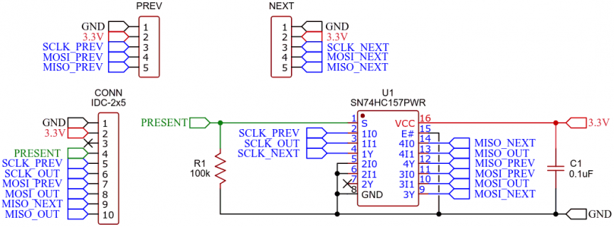
The next simplest solution would be to use a single SN74HC157 chip per socket:
spi-shift-socket.png
The SN74HC157 is a quad 2:1 multiplexer or selector. One of the four channels is not needed here, so the second channel above has both inputs connected to ground. (The output is not connected. You could connect 2I0 or 2I1 to VCC, and 2Y to the microcontroller to indicate whether this particular socket is present or not. It will reflect the actual state.)
Note that in your own circuit, you can choose whatever order for the four multiplexers. Just remember the signal direction for MISO is reversed, so it needs to be handled in the "opposite direction" (wrt. "previous" - module - "next"), as above.

Whenever pin 1 (S) is low, the _OUT signals on the connector are ignored, and we get SCLK_PREV→SCLK_NEXT, MOSI_PREV→MOSI_NEXT, MISO_PREV←MISO_NEXT, thus bypassing the socket. This is the case when the connector is unpopulated or unconnected.

Whenever pin 1 (S) is high, we get SCLK_PREV→module→SCLK_OUT→SCLK_NEXT, MOSI_PREV→module→MOSI_OUT→MOSI_NEXT, and MISO_PREV←MISO_OUT←module←MISO_NEXT.

Note that all three signals, SCLK, MOSI and MISO, are always routed over each chip, so that the signal delays should stay same. Using a single common SCLK will lead to problems, because there is a 100ns or so propagation delay over each chip. (The difference between MOSI and MISO is that the latter has the opposite signal propagation direction.)

You could add an ON-ON toggle switch between the two PRESENT net labels, so that the user can physically control whether a connected module is enabled or not, instead of yanking on the IDC connector.

You can use the unused multiplexer (2I0/2I1→2Y), connecting 2Y to a microcontroller input pin, and 2I0 and 2I1 to VCC and GND, to detect whether the module is present (and enabled) or not.

You can use R1 and the connector PRESENT pin, connected to a microcontroller input pin, to detect the presence of each module; and connect the 74HC157 PRESENT (S, pin 1) only to a microcontroller output pin, if you want to enable or disable each module present via the microcontroller.
 
For pure shift registers:

Let's assume we use three signals: SCLK, MOSI, and MISO.

Each socket receives SCLK_PREV, MOSI_PREV, and MISO_PREV from the previous socket, forwarding them to the next socket as SCLK_NEXT, MOSI_NEXT, MISO_NEXT. (That is, SCLK_NEXT in socket 2 is the same as SCLK_PREV in socket 3.)

On each socket, signals from the previous socket are connected to SCLK_PREV, MOSI_PREV, and MISO_PREV. The corresponding shift register outputs are SCLK_OUT, MOSI_OUT, and MISO_OUT. Note that we do want to route clock the same way we route the two data signals, to ensure they stay in sync. Although eight pins on the socket connector will suffice (VCC/3.3V, GND, SCLK_PREV, SCLK_OUT, MOSI_PREV, MOSI_OUT, MISO_NEXT, MISO_OUT), I suggest adding an additional PRESENT pin, which is connected to VCC on the module whenever the module is enabled. (That is, you can use e.g. an ON-OFF toggle switch to select whether the module is enabled or not.)

When the module is present, we want SCLK_PREV to be connected/shorted to SCLK_NEXT, MOSI_PREV to MOSI_NEXT, and MISO_NEX to MISO_PREV, with minimal resistance (impedance) and capacitance possible. When the module is not present, we want those to be separate.


The simplest solution is to use a "jumper module" for unused sockets, which simply connects SCLK_PREV to SCLK_OUT, MOSI_PREV to MOSI_OUT, and MISO_OUT to MISO_NEXT, and leaves VCC and GND unconnected. (You do not need the PRESENT at all then.)


The next simplest solution is to use a 3PDT toggle switch (like Dailywell 1M31T1B1M1QES from Mouser), with nine pins. The common set of three pins is connected to SCLK_NEXT, MOSI_NEXT, and MISO_PREV. "Off" set is connected to SCLK_PREV, MOSI_PREV, and MISO_NEXT. "On" set is connected to SCLK_OUT, MOSI_OUT, and MISO_OUT. This way, the physical switch selects whether the SPI bus is routed via the module or not.


The next simplest solution would be to use a single SN74HC157 chip per socket:
The SN74HC157 is a quad 2:1 multiplexer or selector. One of the four channels is not needed here, so the second channel above has both inputs connected to ground. (The output is not connected. You could connect 2I0 or 2I1 to VCC, and 2Y to the microcontroller to indicate whether this particular socket is present or not. It will reflect the actual state.)
Note that in your own circuit, you can choose whatever order for the four multiplexers. Just remember the signal direction for MISO is reversed, so it needs to be handled in the "opposite direction" (wrt. "previous" - module - "next"), as above.

Whenever pin 1 (S) is low, the _OUT signals on the connector are ignored, and we get SCLK_PREV→SCLK_NEXT, MOSI_PREV→MOSI_NEXT, MISO_PREV←MISO_NEXT, thus bypassing the socket. This is the case when the connector is unpopulated or unconnected.

Whenever pin 1 (S) is high, we get SCLK_PREV→module→SCLK_OUT→SCLK_NEXT, MOSI_PREV→module→MOSI_OUT→MOSI_NEXT, and MISO_PREV←MISO_OUT←module←MISO_NEXT.

Note that all three signals, SCLK, MOSI and MISO, are always routed over each chip, so that the signal delays should stay same. Using a single common SCLK will lead to problems, because there is a 100ns or so propagation delay over each chip. (The difference between MOSI and MISO is that the latter has the opposite signal propagation direction.)

You could add an ON-ON toggle switch between the two PRESENT net labels, so that the user can physically control whether a connected module is enabled or not, instead of yanking on the IDC connector.

You can use the unused multiplexer (2I0/2I1→2Y), connecting 2Y to a microcontroller input pin, and 2I0 and 2I1 to VCC and GND, to detect whether the module is present (and enabled) or not.

You can use R1 and the connector PRESENT pin, connected to a microcontroller input pin, to detect the presence of each module; and connect the 74HC157 PRESENT (S, pin 1) only to a microcontroller output pin, if you want to enable or disable each module present via the microcontroller.
I'm using the 74HC595 shift register, and the clock and latch pins are shared among all chips, and not daisy chained. What you said about sync might be the culprit. I'm trying out different versions with a modified shiftOut() function, where I can have control over each signal, where I'm applying delays in between. I'm still getting the same results, but do you think it could work if there is a delay between some pulses?
For example, here's the modified shiftOut() function:
Code:
void shiftout(uint8_t dataPin, uint8_t clockPin, uint8_t bitOrder, uint8_t val)
{
    uint8_t i;

    for (i = 0; i < 8; i++)  {
        if (bitOrder == LSBFIRST) {
            digitalWrite(dataPin, val & 1);
              delayMicroseconds(MODULES_SPI_DEL);
            val >>= 1;
        } else {   
            digitalWrite(dataPin, (val & 128) != 0);
              delayMicroseconds(MODULES_SPI_DEL);
            val <<= 1;
        }
            
        digitalWrite(clockPin, HIGH);
        delayMicroseconds(MODULES_SPI_DEL);
        digitalWrite(clockPin, LOW);
        delayMicroseconds(MODULES_SPI_DEL);       
    }
}

void setOutputShiftRegs() {
      digitalWrite(moduleShiftOutLatch, LOW);
      delayMicroseconds(MODULES_SPI_DEL);
      for (int i = NUMMOD - 1; i >= 0; i--) {
        shiftout(moduleShiftOutDataPin, moduleShiftInOutClockPin, MSBFIRST, outputData[i]);
      }
      digitalWrite(moduleShiftOutLatch, HIGH);
}
I'm trying some different values for MODULES_SPI_DEL. Is there any spot where you would change this code?
I'm insisting on the hardware I'm currently using, as I have an assembled PCB that I'm working on. Since speed is not really an issue, I'd rather get this one working, before I start designing the board again.

P.S. I'm using two pins on the IDC that are shorted on the modules, which give a HIGH voltage to a chip on the bus board, so the Teensy can determine whether a SPI signal should be sent to the IDC or whether it should bypass it and move on. This works fine with 74HC165 input shift registers detecting connected modules, and 74HC595 output shift registers controlling the base pins of the transistors. The distances for these chips are longer than the ones I'm trying out with modules, and their traces are thinned (0.15mm), and they work fine with shiftIn() and shiftOut(), so I guess the transistors are doing something funny that might cause this sync problem.
 
Still no idea what the problem with the transistor circuit is as you haven't provided the schematic...
 
Still no idea what the problem with the transistor circuit is as you haven't provided the schematic...
Here's a PDF to the schematic of the bus board. This schematic doesn't include the Teensy, as this is located in another board that connects to this bus board. Anyway, it is a rather complex system, and I don't know if sharing all of it would help. I've attached this schematic.

Chips U3 and U6 are the input shift registers that detect connected modules. The IDC connectors, marked J1 to J19 have 3V3 on pin 19, which is shorted with pin 20, when a module is connected. Pin 20 connects to one of the eight input pins of these shift registers.
Chips U1, U4, U7, and U9 are output shift registers that control the transistors. The transistors are marked with Q. Each IDC connector has three transistors on each side, for three different SPI signals (two input and one output). If a module is detected, the transistors on the left side get a HIGH voltage at their base, and the SPI signals are routed to the IDC connector. If no module is detected in an IDC socket, the transistors on the right side get a HIGH voltage at their base, and the SPI signals bypass the IDC connector and proceed to the next IDC socket.

This is a rough explanation of what is supposed to happen on this board.
 

Attachments

  • output.pdf
    581 KB · Views: 31
Last edited:
I do suspect the issues alexandros is seeing are due to timing mismatch between clock and data signals, as well as noise. Schmitt triggers on input can help with the noise, but to fix the timing issues, both clock and data signals must be routed the same way (with roughly the same length conductors). Where the limits lie for "same" depend on the data rate, and allowed rise/fall times.

Note that for '595, the latch signal does not need to be synchronized with the clock at all: a rising edge on the STCP line latches the output pin states from the internal shift register. (A new bit is read into the internal shift register from the DS pin on the rising edge on the SHCP line, and on the falling edge the Q7S will change to the value of the highest/oldest bit in the shift register.) You can simply wait for the maximum duration of combined latencies after the last falling edge of the SHCP line (so that even the last module will have seen the last falling edge of the SHCP line), and then pulse STCP high for at least 110 ns.

In a very real sense, a SPI bus can be modeled as a pair of shift registers, one in each direction, with a common clock. There is no need to bit-bang the bus, as you can use just one side (MOSI or MISO) of a SPI peripheral; I would consider using two SPI buses here, if both directions are needed.

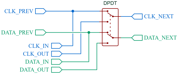
If we look at just one direction, a simple two-pole two-throw switch (6 pins) is needed per module:
shift-switch.png
Note that the above corresponds to SPI SCK and MOSI, and if you add MISO, it is reversed wrt. NEXT and PREV signals (with _IN being the actual input to the module, and _OUT the output from the module), and of course a 3PDT switch (9 pins) is needed.

As I understand it, the Boolean logic needed for NEXT is NEXT = (PREV AND (NOT PRESENT)) OR (OUT AND PRESENT), where PRESENT is asserted when a module is present. (XOR can be used instead of OR, too.) If I read it correctly, the circuit implements the above via
shift-transistor.png
where CTL1 = NOT CTL2. The problem here is that a module present cannot be turned off, because it directly drives the data line to the next module. I was expecting something along the lines of
shift-transistor-2.png
instead, with CTL1 = NOT CTL2 strictly enforced.

My suggestion is to use SN74HC157 instead:
shift-74hc157.png
with clock routed exactly the same as MOSI, assuming PREV is toward master, and NEXT is away from master, and module N's NEXT is module N+1's PREV. On the 74HC157, /G is always low, and A/B is high when the module is in the SPI chain, low when the module is bypassed or not present. You do need a 100 nF = 0.1 µF ceramic capacitor near each '157, between VCC and GND.

Now, because the '157 has four A/B/Y switches in each package, you could use a separate clock for MOSI and MISO, essentially making them separate shift registers in opposite directions. Or, you could have a SPI bus with two signals in one direction, either MOSI1+MOSI2+MISO+CLK or MOSI+MISO1+MISO2+CLK. Note that you then also need half the selector lines; only one per socket (A/B to '157).

The SN74HCS157 (SN74HCS157DR in SOIC-16 and SN74HCS157PWR in TSSOP-16 are 0.38€ or less apiece at Mouser) includes Schmitt trigger inputs, which should add some noise immunity. Adding small-valued resistors in series with the signals can also help, because that way more current is needed to pull a signal high.

I almost always have to iterate my own designs and boards; this (74HCS157 per IDC socket) would be the way I would continue here, considering the observed issues and complexity. I do not know how one could fix the existing board without basically a complete redesign. That is also why I don't see any sense in examining the code that would only work with the current board design; apologies. :cry:
 
Last edited:
I do suspect the issues alexandros is seeing are due to timing mismatch between clock and data signals, as well as noise. Schmitt triggers on input can help with the noise, but to fix the timing issues, both clock and data signals must be routed the same way (with roughly the same length conductors). Where the limits lie for "same" depend on the data rate, and allowed rise/fall times.

Note that for '595, the latch signal does not need to be synchronized with the clock at all: a rising edge on the STCP line latches the output pin states from the internal shift register. (A new bit is read into the internal shift register from the DS pin on the rising edge on the SHCP line, and on the falling edge the Q7S will change to the value of the highest/oldest bit in the shift register.) You can simply wait for the maximum duration of combined latencies after the last falling edge of the SHCP line (so that even the last module will have seen the last falling edge of the SHCP line), and then pulse STCP high for at least 110 ns.

In a very real sense, a SPI bus can be modeled as a pair of shift registers, one in each direction, with a common clock. There is no need to bit-bang the bus, as you can use just one side (MOSI or MISO) of a SPI peripheral; I would consider using two SPI buses here, if both directions are needed.

If we look at just one direction, a simple two-pole two-throw switch (6 pins) is needed per module:
Note that the above corresponds to SPI SCK and MOSI, and if you add MISO, it is reversed wrt. NEXT and PREV signals (with _IN being the actual input to the module, and _OUT the output from the module), and of course a 3PDT switch (9 pins) is needed.

As I understand it, the Boolean logic needed for NEXT is NEXT = (PREV AND (NOT PRESENT)) OR (OUT AND PRESENT), where PRESENT is asserted when a module is present. (XOR can be used instead of OR, too.) If I read it correctly, the circuit implements the above via
where CTL1 = NOT CTL2. The problem here is that a module present cannot be turned off, because it directly drives the data line to the next module. I was expecting something along the lines of
instead, with CTL1 = NOT CTL2 strictly enforced.

My suggestion is to use SN74HC157 instead:
with clock routed exactly the same as MOSI, assuming PREV is toward master, and NEXT is away from master, and module N's NEXT is module N+1's PREV. On the 74HC157, /G is always low, and A/B is high when the module is in the SPI chain, low when the module is bypassed or not present. You do need a 100 nF = 0.1 µF ceramic capacitor near each '157, between VCC and GND.

Now, because the '157 has four A/B/Y switches in each package, you could use a separate clock for MOSI and MISO, essentially making them separate shift registers in opposite directions. Or, you could have a SPI bus with two signals in one direction, either MOSI1+MOSI2+MISO+CLK or MOSI+MISO1+MISO2+CLK. Note that you then also need half the selector lines; only one per socket (A/B to '157).

The SN74HCS157 (SN74HCS157DR in SOIC-16 and SN74HCS157PWR in TSSOP-16 are 0.38€ or less apiece at Mouser) includes Schmitt trigger inputs, which should add some noise immunity. Adding small-valued resistors in series with the signals can also help, because that way more current is needed to pull a signal high.

I almost always have to iterate my own designs and boards; this (74HCS157 per IDC socket) would be the way I would continue here, considering the observed issues and complexity. I do not know how one could fix the existing board without basically a complete redesign. That is also why I don't see any sense in examining the code that would only work with the current board design; apologies. :cry:
Thanks for the detailed answer and ideas! The SN74HC157 seems like a great solution. Also, I didn't think of routing the clock signal the same way as I did with the data signal, which makes total sense as you point out. The MOSI+MISO1+MISO2+CLK scenario is what I need here. I guess I can use the hardware SPI clock pin (13) with another SPI bus, or with software SPI (with shiftIn()), right? This software SPI will run once when the system is powered up, and then the hardware SPI will take over, so there shouldn't be any conflict with the pins used.
A redesign is indeed what's needed here. It will take time, but I'll get back with results when I have designed and printed a new board.
 
Yes that chaining of signals isn't what I was expecting at all - I was expecting just inverter stages to boost current or something. Never seen a BJT used like that, normally wired-OR or wired-AND using diodes is about the limit of mixing discrete with logic chips.
 
Thanks for the detailed answer and ideas! The SN74HC157 seems like a great solution. Also, I didn't think of routing the clock signal the same way as I did with the data signal, which makes total sense as you point out. The MOSI+MISO1+MISO2+CLK scenario is what I need here. I guess I can use the hardware SPI clock pin (13) with another SPI bus, or with software SPI (with shiftIn()), right? This software SPI will run once when the system is powered up, and then the hardware SPI will take over, so there shouldn't be any conflict with the pins used.
A redesign is indeed what's needed here. It will take time, but I'll get back with results when I have designed and printed a new board.
Use one SPI as a master, connected to CLK+MOSI+MISO1. Then, use another SPI as a slave, connected to CLK+MISO2, with MOSI unconnected. Teensy 4.x are all well suited for this.

If you want more parallel buses with the same clock, you could use two SN74HCS157 per socket, for CLK + MOSI1 + .. + MOSIn + MISO1 + .. + MISOm, for n+m = 7. Within each module, the CLK signal is in phase with the MOSI and MISO signals; but as you've seen, they are not in phase across all modules, due to wire lengths and components in the signal path. This you would need to bit-bang, but there is a simple table lookup trick via GPIOn_DR_TOGGLE if all signals are in the same GPIO bank. (That is, you need to use a similar software approach; the hardware SPI buses can use DMA on Teensy 4.x, so you could do other stuff while transferring SPI data back-and-forth.)

(The bit-banging table lookup trick only takes 4×2⁷+4+4 = 520 bytes of tightly coupled RAM, and allows any pins within the same GPIO bank in whatever order to be used, and can even be (re)configured at run time! Let me know if you want further details; I use a variant of this method for wider parallel buses too, especially handling display RGB data, as Teensy 4.x is fast enough to do a bit of computation on each data word while maintaining a pretty high data rate, when bit-banging a bus like this.)

KurtE has created a few documents, including a spreadsheet table of which Teensy 4.0/4.1/MicroMod pins are in which GPIO bank n, and which peripherals they can be connected to, here.
 
Last edited:
Maybe you've already considered signal quality issues, but if not, look for other recent threads where series resistors have been recommended. I recall one about a week ago where 5 SPI chips on the same with a Teensy 4.1 and an "expansion connector" worked fine (at low SPI clock speeds) but then would not work if about 10-12 inches of ribbon cable (with no other chips connected) was just plugged into the connector. While all this type of troubleshooting over the internet involves some guesswork, it's a pretty safe bet the extra wire length added a "long" unterminated stub which created overshoot and ringing due to the very high bandwidth rising and falling edges. Even if you clock slowly, unless you've used series resistors or other ways to limit the slew rate of those fast edges, you can end up with a lot of signal quality issues. The problem are especially severe with 2 layer PCBs where GND isn't routed as an unbroken internal plane directly underneath the signals. Using a many-PCB backplane could end up even worse if not planned carefully.
 
Maybe you've already considered signal quality issues, but if not, look for other recent threads where series resistors have been recommended. I recall one about a week ago where 5 SPI chips on the same with a Teensy 4.1 and an "expansion connector" worked fine (at low SPI clock speeds) but then would not work if about 10-12 inches of ribbon cable (with no other chips connected) was just plugged into the connector. While all this type of troubleshooting over the internet involves some guesswork, it's a pretty safe bet the extra wire length added a "long" unterminated stub which created overshoot and ringing due to the very high bandwidth rising and falling edges. Even if you clock slowly, unless you've used series resistors or other ways to limit the slew rate of those fast edges, you can end up with a lot of signal quality issues. The problem are especially severe with 2 layer PCBs where GND isn't routed as an unbroken internal plane directly underneath the signals. Using a many-PCB backplane could end up even worse if not planned carefully.
Can you give an example of where these series resistors should be placed? Also, how much resistance for each?
 
The series resistor is placed between the IC pin that drives the signal voltage, and the rest of the signal trace.
(If we put the series resistor on the other side, near the input pin, we get reflections and other nasty stuff, because electrical signals propagate at a finite speed.)

You see, logic input pins tend to draw very little current. The SN74HCS157 (HC157 with Schmitt triggers on inputs) sources or sinks a maximum of 2 µA from an input pin, for example. This means that very little noise current is needed to change the signal voltage.

Placing a resistor in series just after the pin that drives it, ensures that much more current is needed to change the voltage level. Noise needs much more power to affect the signal. This means that the same amount of coupled noise would affect the voltage level much less.

As the most crude possible approximation, we can decide the resistor based on the amount of additional current I we want to draw from the driving pin, and how much of a voltage drop V (below what the output pin voltage) we can accept: R = V / I.

A common example I see suggested for SPI would be a resistor of R = 100 Ω. At I = 1 mA = 0.001 A of current, the voltage drop is V = 0.1 V.

(It also provides some protection against having the signal line shorted to ground somewhere after the resistor burning up the output pin, because then the resistor also limits the current drawn from the driving pin to I = V / R. For example, at 3.3 V logic levels, 100 Ω to ground draws 33 mA, and dissipates 109 mW as heat.)

Now, a proper handling of all this would go deep into RF transmission line stuff and things like characteristic impedance of the signal line; as well as into RF/high-speed driving properties of the output pin, like slew rate. All my reasoning here is just the crudest possible approximation, ignoring all the important stuff.

It makes much more sense to start with some reasonable commonly used resistor values (between 10 Ω and 100 Ω for SPI), and use an oscilloscope to look at the actual signals at the corresponding input pin, and adjust the resistor value to see what produces best real-world results, considering the unit-to-unit variances between electronic components. In fact, the real PCB designers do this all the time, because practical reality always trumps theory.
 
100 ohms is a good starting point. Important to place it close to the transmitter.

If using a 4+ layer PCB that has an unbroken ground plane directly underneath the traces and especially with wider traces, you might want a somewhat lower resistor like 75 or 50 ohms. But for minimum width traces, you probably want around 100 ohms.

If using a 2 layer PCB, put extra effort into routing GND alongside SCK, and also keep MOSI close if you can. The best case scenario isn't anywhere close to what you'll get with an unbroken ground plane inside a 4 layer PCB. Theoretically your wiring probably wants quite a bit higher than 100 ohms, especially if you can't always keep GND close. But a much higher resistor can also form a low-pass filter with the capacitance of the pins of all connected chips, so in practice you're probably limited from using the "ideal" resistor. Bottom line is 2 layer boards (or 4 layer with a broken ground plane or no ground plane) gives poor signal quality for high speed digital signals. 100 ohms or perhaps slightly higher can make the best of a bad situation, but don't fool yourself into thinking it'll ever be really good (a common thought many people have after pouring so many hours into difficult routing... the electrons and the fields they create don't care how much time you spent routing). You just can't get GND consistently very close to high speed signals with only 2 layers. Best you can do is route GND alongside signals and use 100 to maybe 220 ohms and accept the trade-off in signal quality comes with the lower PCB cost.
 
Last edited:
100 ohms is a good starting point. Important to place it close to the transmitter.

If using a 4+ layer PCB that has an unbroken ground plane directly underneath the traces and especially with wider traces, you might want a somewhat lower resistor like 75 or 50 ohms. But for minimum width traces, you probably want around 100 ohms.

If using a 2 layer PCB, put extra effort into routing GND alongside SCK, and also keep MOSI close if you can. The best case scenario isn't anywhere close to what you'll get with an unbroken ground plane inside a 4 layer PCB. Theoretically your wiring probably wants quite a bit higher than 100 ohms, especially if you can't always keep GND close. But a much higher resistor can also form a low-pass filter with the capacitance of the pins of all connected chips, so in practice you're probably limited from using the "ideal" resistor. Bottom line is 2 layer boards (or 4 layer with a broken ground plane or no ground plane) gives poor signal quality for high speed digital signals. 100 ohms or perhaps slightly higher can make the best of a bad situation, but don't fool yourself into thinking it'll ever be really good (a common thought many people have after pouring so many hours into difficult routing... the electrons and the fields they create don't care how much time you spent routing). You just can't get GND consistently very close to high speed signals with only 2 layers. Best you can do is route GND alongside signals and use 100 to maybe 220 ohms and accept the trade-off in signal quality comes with the lower PCB cost.
If I switch to four layers, does this mean that all modules that connect to this bus board must also have four layers with an unbroken ground?
 
Back
Top