This is a new project. First articles are out for quote at the FAB house now. If anybody would like one of the boards, please let me know as soon as you can. Schematics and discussion are posted to github at the following link. I think it is a pretty fantastic sensor and I am excited to start using it for my research.
https://github.com/drmcnelson/S11639-01-Linear-CCD-PCB-and-Code
The Hamamatsu S11639-01 is a high sensitivity linear CCD. The specs are 20uV/e-, and a dynamic range of 10,000. Ibsen calculates the quantum efficiency at about 0.8. That is 8 to 10 times more sensitivity and 30 times the dynamic range of the low cost linear CCDs. But it is also a lot more expensive. There are a few on ebay for about $400. Fortunately the BOM for the board described here and posted to github is only $50 (current prices at Digikey). Just add sensor and your favorite host capable of SPI (a Teensy 4.0, of course).
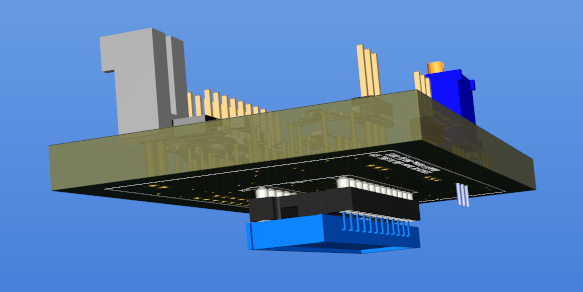
Here are some 3d renderings from the CAD package. Sensor signals and SPI are in the header at the top. VD is the supply for the external side of the logic converters and the SPI side of the ADC, it can be the 3.3V provided by the Teensy. The analog section converts the signal to differential for the 16 bit ADC for a free gain factor of 2. There is an offset for the second stage that is adjusted by the trim pot. The Vref and power for the analog section can be jumpered to the internal supply (4V) or supplied externally.
Last edited:

