SPI Data in/out naming clarity

Status
Not open for further replies.

stevech

Well-known member
I found this info helpful - in the confusing naming of SPI data in/out pins. Teensy uses the DOUT and DIN names, which are somewhat ambiguous as to data direction (sender/receiver perspective).
The "Official" names remove the ambiguity: MISO and MOSI.
Alternative naming conventions are also widely used:

SCLK : SCK, CLK.
MOSI : SIMO, SDO, DO, DOUT, SO, MTSR.
MISO : SOMI, SDI, DI, DIN, SI, MRST.
SS : nCS, CS, CSB, CSN, nSS, STE, SYNC.
 
Last edited:
I think DOUT and DIN are better for beginners\Newbies as they will get confused with MISO and MOSI. I mean they would not know that MOSI(Master OUT Slave IN) and a MISO(Master IN Serial OUT) as these are basically technical names and of relevance once the programmer has knowledge of the SPI Protocol and they will need to actually understand the SPI protocol for this. So to keep it simple it is kept DIN and DOUT.
 
SPI.PNG
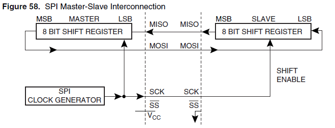
I could not get your question.. DIN corresponds to MISO(Master IN Slave OUT) and as far as the circuits, I have used MISO is connected to MISO of Slave and same with MOSI , also DOUT Corresponds to MOSI. So, I don't think we need a frame of reference for DIN or DOUT. That is the beauty of SPI you don't need criss-cross connection in SPI like we need in UART/USART(TX to RX and vice-versa).Please Refer to screen shot above taken from atmega 8 datasheet. It gives a very clear picture of the interconnection between master and a slave in SPI protocol.
 
I agree completely - with the MISO/MOSI terms as rightfully sown in the diagram. But when SDI/SDO/DIN/DOUT terms are used..

In looking at the wiring between device A and B for a current project, device A labeled the two data pins SDI and SDO and device B had pins labeled DIN and DOUT.

Is it uniformly the case that the Input and Output within SDI/SDO/DIN/DOUT is 100% always w.r.t. the device declaring the name?

Seems to me if everyone used MISO/MOSI there'd be no potential confusion.

Or am I over-thinking this, pondering how to wire A to B and not guess.
 
Last edited:
thanks... My posting was intended to be general, not project specific. I've used SPI in the past but the devices always were marked MISO/MOSI per the de facto standard (Motorola). I'm OK with this for the current project.
Here's a diagram showing the naming aliases and variations. It would be so nice if the industry would consistently use only the original names: MOSI/MISO and SS. Ideally, SPI and I2C would long ago have been taken as IEEE/ISO standards.
Below, note the naming variants in parentheses. DIN, DOUT aren't shown.
SPInaming.JPG
 
Because they are in a datasheet. Only few Engineers or Experienced Electronics person who really work with the SPI protocol can understand it . Here we just have a library that makes the SPI work, I mean again as, I have talked earlier people don't care about what is happening at the register level and to understand the terminology of SPI protocol(MISO and MOSI) they would have to understand the protocol. Anyways, I think if you want the original names(MOSI and MISO) they can still be found using the datasheet to find the pin diagram of the controller and finally mapping it onto Teensy. I also agree these should be already made IEEE/ISO standards. Its been since a long time we are using these protocols and they must be made standard to avoid confusion and multiple names.
 
SPI data In/ SPI data Out is not confusing in my view. In a SPI bus the information flows in a well defined sense, thus SPI OUT pin would be the "SPI emitter" and SIP IN the "SPI receiver"

SPI data Out is the pin/wire through which the information exist from a device and SPI data In is the pin/wire by which the information enters a device.

A SPI bus is a ring o circular bus built by several “daisy chained” shift registers. This is equivalent to a circular register that rotates a bit per clock. Each device “sees” a piece of the circular register composed of 8 bits.

To see this more clearly, let us build a SPI “daisy chained” bus. Say 4 devices located in the dial of a watch: the 12 o'clock device, the 3 o'clock device, the 6 o'clock and the 9 o'clock device.

We need to wire together the 4 devices but first we need to decide the direction of flow of the information in the bus, as SPI bus is a “one sense” bus. Say we choose clockwise.

We first put a wire from SPI OUT of 12 o'clock device to SPI IN in 3 o'clock device. Then a wire from SPI OUT of 3 o'clock device to SPI IN in 6 o'clock device. Then a wire from SPI OUT of 6 o'clock device to SPI IN in 9 o'clock device and finally a wire from SPI OUT of 9 o'clock device to SPI IN in 12 o'clock.

Each pulse of the clock, the 32 bits (4x8) circular register rotate 1 bit clockwise. The bit that overflows from “the right” of the shift register 12 o’clock exits device 12 o’clock through SPI OUT (12 o’clock), travels through the first wire, enters 3 o’clock device through SPI in (3 o’clock) and is injected on the “left” side shift record of 3 o’clock device. The bit that overflows from 3 o’clock register is sent to 6 o’clock register, etc

Each device can read/write in the 8 bits “in front” of it, and then the clock pulses will make travel this bits elsewhere in the circular register where other devices will be able to read/write it.

The number of clock pulses (sent from “master”) determines how many bits will rotate the wheel between reads/writes (“chip select” signal from “master”) but the direction of rotation, which is “one sense”, is “hardwired”
 
Last edited:
Paul pointed out recently that Teensy 3.x can be used in SPI slave mode; DIN is still an input and DOUT is still an output.
 
Nantonos: Yes, they will be same(Would request you to please go through the datasheet of atmega 8 about SPI protocol it has a very nice explanation and also the same is applicable to teensy because the protocol remains the same) and
Thank you FAlameda for the nice explanation. I hope it will be very helpful to newbies but, I think you went a little wrong from the 3rd last para. Actually in SPI by using the CS(Chip Select) you first choose the chip you want to communicate with and then the bits start following so its always 8bit(1x8) ofcourse that again depends upon the architecture. Also in the last para, I think the direction changes when the master takes input from the slave.
 
Well, yes, things can become quite complicated but the essence of a SPI bus is a circular register or loop and viewing it as a circle helps to understand its operation.

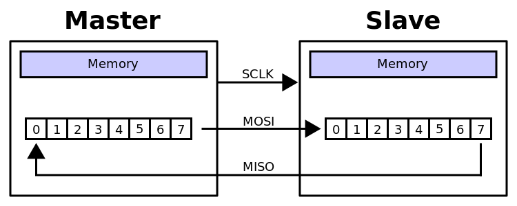
In this image from wikipedia
750px-SPI_8-bit_circular_transfer.svg.png

we can see that even in the simplest case, a master and a slave, the bus is actually a circle or loop. There is no a master sending data to the slave nor a slave responding to the master but both things at the same time. When a tick occurs, the master transmits a bit to the slave and the slave also, at the same time, transmits a bit to de master. When 8 ticks of the clock have occurred, the content of the registers inside the master and the slave have been swapped.

We can expand this SPI bus adding new devices these new devices must be inserted in the “daisy chain”. We cut the loop and insert the new device.

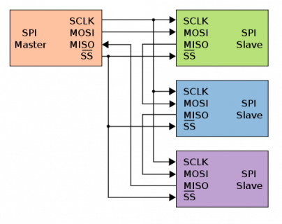
This other image from Wikipedia
500px-SPI_three_slaves_daisy_chained.svg.png

shows a “daisy chained” circular SPI bus. The MOSI/MISO or in/out pins form a big loop and there is only one clock and one “chip select”

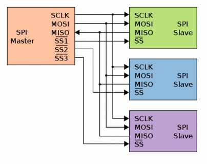
This final image from Wikipedia
500px-SPI_three_slaves.svg.png

shows a typical “tree” SPI, with a master and three slaves but if you look closely you will see that this is not a SPI bus but three superimposed independent SPI buses.

These busses can only be built if the devices have tri-estate pins: high, low and “high impedance” or effectively “outside the world”. When the master selects one of the multiple “chip select” line, the master is allowing only one of the SPI bus to exists and the other devices are really disconnected from the circuit (in high impedance state)

So that this configuration allows the master build in “run time” a circular SPI bus with a master and a slave and hide the other two inactive or “missing” alternate buses.
 
Late arrival here. If I'm reading the specs correctly, MISO/MOSI pin designations are NOT equivalent to DIN/DOUT.

Yes, there would be a 1:1 correspondence between these designations if the device is being used as the master (DIN=MISO/DOUT=MOSI). However, the opposite becomes true if the device is being used as the slave (DIN=MOSI/DOUT=MIS).

If my analysis is correct, this is a very important distinction, because it affects which pins to connect together. In a MISO/MOSI system (as shown several times above), the MISO pins on the master and slave are connected together, and the the MOSI pins are connected together; in other words, the data direction of the pins on the slave is reversed from the data direction on the same pin in the master.

However, in a DIN/DOUT system, the data direction of each pin does not change between master and slave, and the pins must be cross-connected--the DIN pin on the master would be connected to the DOUT pin on the slave, and the DOUT pin on the master would be connected to the DIN pin on the slave.

I'll leave it to future posts to describe how to connect the pins the cases where one chip uses MISO/MOSI and the other uses DIN/DOUT (hint, the wiring changes, depending on which device is master and which is slave).

I am working on a project where two Teensy 3.1's will be connected together via their SPI ports, so I'll find out if my analysis is correct pretty soon!
 
MISO means Master's INPUT, Slave's OUTPUT.
MOSI is the opposite.

DIN, DOUT and as in RS232, RXD, TXD, are confused because it's an implicit "with respect to.." for in and out.

If I had a dollar for every hour lost to head scratching and rewiring due to leaving it implicit!
 
This discussion seems to be circular and the answers have already been given.

Is it uniformly the case that the Input and Output within SDI/SDO/DIN/DOUT is 100% always w.r.t. the device declaring the name?
It is for Teensy and it seems that it is for all/most devices.

Seems to me if everyone used MISO/MOSI there'd be no potential confusion.

Which is what I used to think as well, but as I pointed out in this thread, Paul explained that this was not correct.

Paul pointed out recently that Teensy 3.x can be used in SPI slave mode; DIN is still an input and DOUT is still an output.
Possibly that was a bit terse so let me expand it. With Teensy as SPI master, DOUT is MOSI and DIN is MISO. However, the pinout can't use those terms because in SPI slave mode, DIN is MOSI and DOUT is MISO. In both cases, DIN is an input and DOUT is an output. Thus, the pinout uses those labels because they are always true.
 
I don't have a problem with the names or the logic of the SPI signal directions, but I would like to know if 1) Teensy 3.1 has more than one hardware SPI port and 2) if not, how can more than one device use the Teensy 3.1 SPI pins at the same time without colliding, and 3) how can one configure other pin groups to support 'software' SPI on Teensy 3.1. Is there a thread already that discusses these issues? Thanks!
 
but I would like to know if 1) Teensy 3.1 has more than one hardware SPI port

TL;DR = there's only one SPI port.

The chip actually has 2 in the silicon, but the 2nd port doesn't have SCLK available on any pin, so it's really not usable.

and 2) if not, how can more than one device use the Teensy 3.1 SPI pins at the same time without colliding,

Today: assert only one chip select signal at a time, and never use SPI from an interrupt. The vast majority of SPI devices use MSBFIRST and SPI_MODE0 and work up to fairly high clock speeds. If one or more of your devices needs incompatible settings, you may need to reconfigure the SPI before using each device. Kludgey as this scheme sounds, it's worked remakably well for many years of Arduino's history. Only recently have SPI-based radio modules started requiring interrupts.

Future: use SPI.beginTransaction() before you use the SPI port, and SPI.endTransaction() when you're done and other libraries are allowed to use the port. If you ever access SPI from interrupts, call SPI.usingInterrupt() to register that interrupt with the SPI library.

and 3) how can one configure other pin groups to support 'software' SPI on Teensy 3.1.

Obviously this is only possible if your code or the library you're using has code inside to do bit banging instead of real hardware SPI. Many of the Adafruit libraries have this option. ILI9341 would be just one of many examples. Typically, Adafruit provides 2 different constructors, where you the one you want. The details are up to the author of that code, so refer to the documentation or examples for those libraries to see how this is done.
 
Thank you for the info; it is very useful.

I plan to use the SPI port with the nRF24L01+ and nRF51822 radios, they can be used without requiring interrupts.

BTW, is 'future' months or years?

Lastly, I hope you are considering making the 2nd SPI port operational on the Teensy 3.1++ in the works!
 
BTW, is 'future' months or years?

It's right now, if you're savvy enough to grab the work-in-progress code from github.

https://github.com/PaulStoffregen/SPI

and the libraries I've ported so far (see my github repo list)

In about 1-2 weeks, I'm hoping to publish Teensyduino 1.20-rc2, with this SPI library and all the libraries ported so far. By then, I should have at least SD and several others.

Eventually, an official 1.20 release will be made.

In about 3+ weeks, I'm planning to submit all this as a pull request to Arduino. Cristian has already given tentative approval, but also stated this is a huge change for Arduino to consider. I have no idea when/if they'll publish it in 1.5.8, or 1.5.9, or ....
 
Back to esoteric-ville... I guess the one advantage of the MISO/MOSI convention has over the DIN/DOUT is in schematic/board layout. You can actually name the line that goes between MISO pins "MISO", for example. You can't do that with DIN/DOUT because DOUT winds up going to the other chip's DIN pin, so naming the line would be ambiguous. Paul, I like your MISI/MOSO comment :)
 
Status
Not open for further replies.
Back
Top