16ch CV out project

elgiano

Member
Hello!
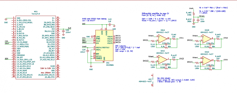
I'm starting a project in which I need 16 CV out channels, with a teensy 4.0. I was thinking about using two PCM1681 DACs, and I have a few preliminary questions:

1. Any comment or advice about components or design is super welcome!
2. Shall I use the two I2S ports on the teensy to communicate with DACs? In this case shall I make a class that does what i2s2 is to i2s, but for i2s_oct, or is there a simpler method?
3. Or shall I use AudioOutputTDM? In this case can I use any PWM pin to send data to DACs data ports?

Thanks! I come from software development, and although I have made several electronics projects with teensy for "control data", this is my first time with analogue audio.

If anyone is interested in more context about the project, it's a digitally-controlled analogue no-input mixer: I want to send OSC over serial to teensy to generate control voltage for VCAs in a matrix mixer. The mixer has 2 channels, each with a 3-band eq, that feedback into each other and get mixed into a main bus, which also feedbacks into each channel. Each channel also has an external insert. So there would be 8 cvs for each channel: insert, fb_main, fb_1, fb_2, eq_l, eq_m, eq_h, vol. Thus, the requirement for 16 cv outs.

Thanks to anyone who would like to help me kickstarting this!
 
Thanks for the super quick answer!

Sorry I don't exactly know what you mean with DC accuracy. If it's about generating an accurate DC voltage so that I can sustain a CV value, then the answer is yes, or better, it depends on how much inaccuracy I can live with I guess.
Would you have any other ideas than DACs to supply CV parameter control? In the end I would like to have like a knob, except that is a computer turning it.
 
For CV out you do need DC accuracy which means audio DACs are not a good choice. Have a look at something like the DAC8568 from Texas Instruments; it gives you eight reasonable quality 16-bit outputs (4LSB INL, 0.004% typical Initial Accuracy), has an internal voltage reference that is good enough for this application, and is driven by SPI. Two of those would give you 16 channels of CV out.
 
Great, thank you!
I was looking at these DACs, found some other threads on this forum and the o_c module that does precise CV with teensy3. I was also looking at version that are equally precise, but without internal reference. Could you explain me a bit how the internal reference works and how am I supposed to use it?
1. datasheet says internal reference is at 2.5V. Is this regardless of power supply voltage? Does it also mean that the DAC will always output values between 0 and 5v when using internal reference?
2. can I feed this reference to the VCA (looking at SSI2164) so that it will "understand" this CV properly? and will this mean that the VCA would also output values between 0 and 5v then?

EDIT: maybe I rushed a bit: if I give Vref from DAC to VCA, assuming CV ranges between 0 and 5V, then a CV of 5V will give a gain of +20dB, that corresponds to 10 times the voltage of the input. Is this right?
 
Last edited:
Normally you connect an opamp to each the DAC output pin. The opamp allows you to boost (and also offset if needed) the signal so you get the desired voltage range. It also provides a strong (or lower impedance) signal.

The opamp can also add noise and voltage offset (error), so you would usually want to chose a good one. Offset error can be calibrated, either by adjusting the numbers before sending to the DAC, or by an analog circuit, so normally you would focus mostly on low noise and offset error which doesn't vary much with temperature.

If using the internal reference, normally you would only connect capacitors to the DAC's reference pin. You might also connect the reference voltage, perhaps through resistors, to your opamp circuitry. But generally you want to avoid placing any sort of load on the reference voltage. It's not meant to be a signal output. The accuracy of your signals depends on the reference.

High quality DACs, even ones like this which have a very good reference build in, usually give you an option to connect an external reference which is presumably even better. Ultimately the DAC's voltage output is proportional to the reference voltage. If you shop for reference voltage chips on TI or Analog Devices websites, you'll see they make many different parts with varying levels of initial accuracy and temperature stability.
 
Thanks for your tips and patience! I'm doing little steps, but one after the other, I'll hopefully get somewhere!

My current understanding of this "mapping" problem is:
- VCA has a -33 mV/dB gain constant, and gains from -100dB to +20dB. This translate to an expected CV range between -0.66V and 3.3V, where 0V = 0dB (unity gain)
- different DACs have different specs, but I see two patterns so far: class A and B, which output from 0 to Vref, and class C and D, which output from 0 to 2*Vref
- I can use a differential amplifier to map from DAC's output range to VCA's CV range
For this i connect the DAC internal reference to the op-amps. Although this could be a problem according to Paul's last comment, I've seen this done in other schematics and from what I understood of datasheets it looks like it's supposed to be an output (but perhaps here we mean different things when we say output?).

I made a reduced schematic, with a 4 channels DAC8565, which apart from the number of channels should be equivalent to DAC8568. If anyone could have a look and give me any feedback, it would be very appreciated!

Note: I didn't include the VCA yet, and I didn't figure out a power solution yet.
output.jpg
 

Attachments

  • output.png
    output.png
    88 KB · Views: 129
Last edited:
I see a mistake already: DAC8565 outputs up to 5V, so it needs at least 5V (6?) as AVdd, right? On the other hand DAC8568 outputs up to 2.5V, so could I power it from the 3v3 from teensy?
 
You would use a 5V supply (like V USB) to power the DAC and a level translator like 74AHCT125 to convert the 3V3 Teensy logic to 5V0. You would also need something like 4.7μF + 100nF supply bypass caps on AVdd.

DAC8568C outputs up to 5V (2 * Vref) and has a zero-scale reset.

Do you really need to drive the VCA beyond unity gain? Typically in analog synths, a VCA is used only as an attenuator, not to add positive gain? Then you wouldn't need the differential op-amp parts (there are already output buffers built in).

I haven't designed anything with 2164 VCAs so can't really offer advice there but I had a few notes stored away that might be useful:

- https://www.njohnson.co.uk/index.php?menu=2&submenu=2&subsubmenu=3
- https://modwiggler.com/forum/viewtopic.php?p=816108&sid=cb90adb57dd34a46dfbac2ee0460625e#p816108
- https://modwiggler.com/forum/viewtopic.php?p=2685546#p2685546
- https://electricdruid.net/multimode-filters-part-2-pole-mixing-filters/
 
Last edited:
DAC8565 outputs up to 5V, so it needs at least 5V (6?) as AVdd, right?

On page 3 the datasheet says it outputs 0 to Vref.

screenshot.png

The built in VREF is 2.5V.

The first page of the datasheet says the power supply range is 2.7 to 5.5 volts.

screenshot.png

On page 3, it also says the input range if using external VREF is anything between half the power supply to all the way up to your power supply voltage.

So you could use an external VREF and power it with slightly higher than 5V, but going to 6 volts would exceed the allowed range. But that's just one particular usage case. The typical use would be 2.5V output using the internal reference. To assume DAC8565 always outputs 5V range ignores all this info printed in the datasheet.
 
Hey, thanks for all the information and help, I'm still working on it.
While I wait for the DACs to arrive, I'm writing the SPI code. Could you have a look at this snippet and see if it looks all right? My only doubt is because I'm transferring chunks of 24 bits, I've never used the SPI library before, I don't have access to a logic analyzer, and I couldn't try it with the DAC yet.

This code is meant to set one channel of a four channel DAC8564

Code:
// datasheet says: MSB_FIRST, sampling on falling edge, so mode 1
SPISettings spiSettings(50000000, MSB_FIRST, SPI_MODE1);

uint8_t addr = 0b00; // device address when both ADDR pins are grounded
uint8_t load = 0b01; // 01 means update this channel
uint8_t ch = 0b01; // channel number 1 (channel B)

// 8 bits: A1 A0 L1 L0  - C1 C0  -
//          0  0  0  1  0  0  1  0
uint8_t ctrl = addr << 6 | load << 4 | ch << 1;
// 16-bit DAC value
uint16_t val = 0xff00;

// send 24 bytes, ignore MISO
SPI.beginTransaction(spiSettings);
digitalWrite(selectPin, LOW);
SPI.transfer(ctrl);
SPI.transfer16(val);
digitalWrite(selectPin, HIGH);
SPI.endTransaction();
 
Other than the settings, which are easy enough to experiment, this code looks like it should work.

I would recommend using a much slower clock, at least while you're doing first testing. Best to get it working first slowly, then increase speed after you know it's stable with slower supply. You might also try SPI_MODE0 if SPI_MODE1 doesn't work.

Technically (according to NXP's official specs) 30 MHz is the maximum supported SPI clock speed. Anything higher is considered overclocking. Many people have reported success with higher speeds on some devices, especially TFT displays.
 
Hello!
Just wanted to share with you that everything works! Thanks for all the inputs and comments!
Technically (according to NXP's official specs) 30 MHz is the maximum supported SPI clock speed. Anything higher is considered overclocking. Many people have reported success with higher speeds on some devices, especially TFT displays.
Now I'm running at 1MHz: I have a problem with digital bleed and running at lower speed helps reducing it a lot. What happens is that when I amplify a lot in the VCA, I can hear switching noise whenever I send SPI data, even when not changing DAC values (i.e. setting them to the value they already had). I guess I need to spend time figuring out the return current paths, but my circuit analysis skills are close to zero, and anyways running at lower speeds makes it almost bearable... so if anyone has any tip on this I'd be happy to hear it, but I guess it's a more complex issue that what I can bother you with :)

For now I'm happy to share my schematics for the DAC+VCA part, and also for the "motherboard" circuit that puts them together into my first prototype of this digitally controllable analogue no input mixer! Thanks again for everything!!
 

Attachments

  • DCA_rev1_schematic.pdf
    78.7 KB · Views: 70
  • anim_rev1_schematics.pdf
    181.8 KB · Views: 61
Back
Top