I photo etched a lot of PCBs in the 1990s. Made a light exposure table with UV florescent tubes in 1989, and even built an "acid swishing machine" in 1992 with the stepper motors from old 8 inch floppy drives that held a Pyrex pan with some janky particle board bracket I made.
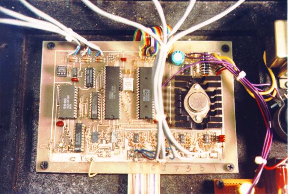
This MIDI drum machine in 1991 was one of the earlier boards.
Gave away all that gear and chemicals in the early 2000s, when a local PCB shop (now
Sunstone) started offering 1 day turn for $80.
Advanced Circuits had been offering "$33 each" back then too, but it always had gotchas like min qty, setup fees, spending shipping. Then Sparkfun started
Batch PCB and the local a guy at the DorkbotPDX meetup started a regular group order that later became
OSH Park, and eventually lots of Chinese companies appeared with super cheap PCBs. Even when it was just 1 company at $80, messing with the chemicals and drilling holes and having to solder wires into every via just lost its appeal.
Today I still mostly use OSH Park for prototypes and sometimes the Chinese companies for larger boards or when I need more than just a few.
If you really want to mess with the chemicals, the way I usually used was pre-coated boards, like this:
https://www.amazon.com/GC-21-334-VP-Positive-Pre-Sensitized-Single-Sided/dp/B01N5W07AM
You can get the photoresist chemical and bake it onto bare copper PCB material (did that too in the early days) but the photoresist chemical emits a lot of fumes during the baking process. Very difficult to get a uniform coating. With all the other stuff that tends to go wrong along the way, best to start out with pre-coated material.
Early on I printed onto transparency sheet (used with ancient overhead projectors...) but later switch to vellum paper. It lets less light through, so you have to expose to the UV light longer, but laser printer toner prints onto it much better. By the mid-1990s I was regularly making 10 mil lines with 10 mil spacing (approx 0.25 mm) with good success. Vellum paper really helped. I also had 2 pieces of 1/4 inch thick glass I would put on below and on top, with their weight pressing the paper to the PCB.
I used to also flip the image before printing, so the toner side of the paper would touch the photoresist. Avoiding the paper thickness between the toner and photoresist made noticeable improvement on small traces. Ideally the UV light would br collimated. I've heard of people placing a few layers
egg crate material painted flat black between the light and PCB under exposure to filter away off-angle light. But I never had such a setup, just 4 fluorescent tubes in a home-made box mounted a few inches above a pull-out shelf which held the glass & PCB sandwich.
Getting the 2 sides aligned was always a challenge. Usually I would tape the sheets together, then slip the PCB material between and tape it on only 1 side. With practice, I could usually get them aligned within better than half the smallest via size (which I believe was 30 mils... but it's been quite a while).
How long to expose was a matter of guesswork.
After exposing, a developer chemical (a strong base) dissolves the photoresist that got exposed to UV. Fortunately from this point on you get visual feedback as you see the colored photoresist wash away, so less guesswork.
Then wash well in running water, and then put it in the acid to etch away the exposed copper. This part takes a lot of patience, which I why I built that janky acid swishing machine so long ago. It goes faster if you heat the acid. If any of the prior steps weren't done quite right, you get a tempting view of your PCB artwork appear and then start to partially vanish, or the exposed copper never seems to fully etch away away.
Drilling all the holes is simple in concept, but tiny drill bits (at least in the 1990s) come in 2 types, carbide which break with even the slightest lateral movement of the PCB while bit is in contact, and high speed steel which dulls quickly when drilling PCB fiberglass.
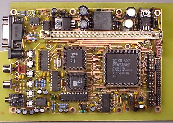
The old
MP3 player project (long before Apple made the iPod) is one of the last PCBs I made this way.
Before you solder, the photoresist needs to be removed. I never found any chemical, always just scrubbed the board with steel wool. There is also a tin plating chemical you can use. As I recall, it was expensive, so I usually just left the photoresist layer on the PCB until right before soldering. The freshly scrubbed copper would solder well for about 12 hours, but quickly start to tarnish.
For many years I used to make at least a few PCBs every month this way, sometimes many more. I gladly gave it all up just as soon as it was easy and inexpensive to just order them online.