On the pinout reference card, I had to make some compromises for the sake of simplicity and limited space. So the 5 data signals are labeled "IN1, OUT1A, OUT1B, OUT1C, OUT1D", which implies the mode of stereo input and 8 channel output. 1 of these 5 is on a bottom side pad, because again so many difficult trade offs were required in assigning the pinout.
Shouldn't this be labeled as SAI1A, SAI1B, SAI1C, SAI1D, SAI1E, and SAI2IN SAI2OUT? For my project I'm going to be converting some of the outputs as inputs. The OUT1A, OUT1B, OUT1C, OUT1D can be either in or out. However, I'm pretty sure the SAI2 is fixed as an in/out combination (no option for switching them to out/out or in/in), unless I'm mistaken. I also know this is not necessarily supported in software yet.
===============
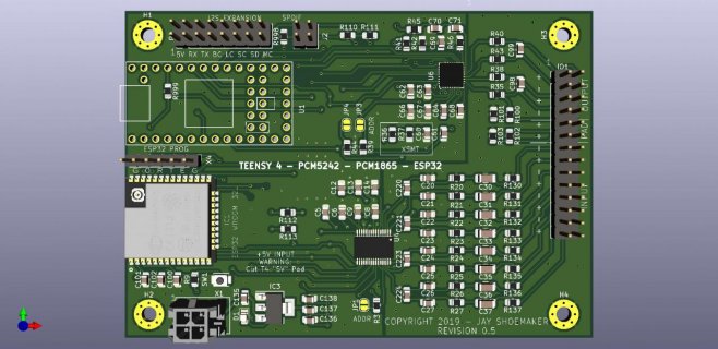
I just completed a design of a board. I had some success with the breadboard, but loose wires are causing me pain. So i'm going to PCB now and I'm antsy to give it a go. I'll probably order the board later today. I have PCM5242, PCM1865, and ESP32WROOM all on one 4-layer board. There is also an expansion header for the SAI2 ports for future testing. Here is how I have it hooked up.
PCM5242 (balanced/single ended output x2)
- CLOCKS 1 (BCLK1, LRCLK1, MCLK1)
- DATA OUT1A
PCM1865 (balanced/single ended input x4, with mic pre)
- CLOCKS 1
- DATA1 = IN1 (CHANNELS 1 + 2 OF PCM1865)
- DATA2 = OUT1D (PLANNED FOR INPUT AS OPPOSED TO OUTPUT, CHANNELS 3+4 OF PCM1865)
ESP32 (A2DP input or output, not simultaneous)
- CLOCKS 1
- DATA FROM ESP32 TO T4 = OUT1C (WHEN SINK, RECEIVING BT-AUDIO IN, INPUT ON TEENSY)
- DATA TO ESP32 FROM T4 = OUT1B (WHEN SOURCE, SENDING BT-AUDIO OUT)
EXPANSION HEADER
- CLOCKS 2 (BCLK2, LRCLK2, MCLK2)
- DATA OUT = OUT2
- DATA IN = IN2
On the breadboard I've confirmed that the PCM5242 hooked to OUT1A, and the PCM1865 hooked to IN1 is working with the audio passthrough sketch. The rest is unconfirmed but like I said, the breadboard is causing issues. I'm hoping that when this board is built I'll get at the very minimum 2 channels output and 2 channels input working with stability. Then the other two input channels, and the ESP32 will be a project that will require software. Hopefully it's hooked up right at least.
I included a footprint for a 100OHM resistor on both MCLK1 and MCLK2. I'm not sure if it's needed or not. It also seems that there might be a way to "adjust" the MCLK levels in software instead of the resistor?
Once I finish staring at the layout and schematic a little longer I'll order the board and start putting it together for testing. I found a few errors this morning, after about a month or more of designing it (and years of research). I guess sometimes you just need to hit "print" and keep your fingers crossed.


