Issue with high-speed bit-banged SPI on Teensy 4.1

rava

Member
Hi everyone,

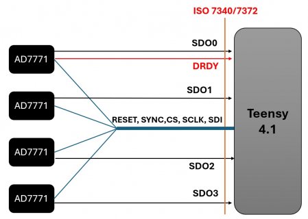
for a university project I am trying to implement simultaneous readout from multiple AD7771 at high speed without using an FPGA (learning curve and time commitment too high). The idea is to use the Teensy 4.1 to implement SPI by bit banging, request data from the ADCs by shared SPI inputs (to the ADC) and read simultaneously by separate output lines. All ADCs are synchronized by using the same local clock source and RESET/SYNC pins so all the data becomes available at the same time. SPI signals are passed between ADCs and MCU through isolators (ISO7340/7342) due to project requirements.

I had a PCB made and wrote some simple Teensy code, where I wait for an interrupt from the DRDY pin on the first ADC, then read data from all channels through SPI and stream it to PC through serial/USB.

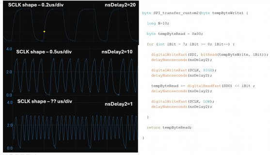
I achieved correct readout on the first ADC at relatively slow SPI by placing small delays (delayNanoseconds) in the code after every digital read/write, but need to go much faster to push through all the data before consecutive ADC readings. Supported speed is 30MHz for AD7771 and 25Mbps for the ISO7340/7342. To clarify, Teensy would be fast enough for my purpose (all SPI comm within 20us) with no delays but in this conditions readout is broken. Problem is, when I reduce or remove the delays in the code, readings become rubbish or flat out zero. I checked the digital signals post-isolator (ADC side) and found the shape of the SCLK signal seriously degrades with increasing speed (see image). Other SPI pins are fine. The SCLK signal tends to shrink in amplitude and get closer to the VDD/2 value (VDD=3.3V).

I understand this is not an issue directly related to the Teensy, especially since the isolator is involved, but I was wondering if I am missing something or there is something I can do on the MCU side to improve clock shape while maintaining high-speed and no delays in code? Please see attached images for further explanation.

Any advice is appreciated. Many thanks.
 

Attachments

  • Img01.jpg
    Img01.jpg
    313.8 KB · Views: 53
  • Img02.jpg
    Img02.jpg
    99.9 KB · Views: 60
With manual control of the pins - not the SPI hardware ? - look into setting the slew rate higher for faster rise time?
 
With manual control of the pins - not the SPI hardware ? - look into setting the slew rate higher for faster rise time?
Thanks! Yes I need to use manual controls so I can read the data from 4 ADCs at the same time. Basically the same "manual" SPI read instruction will feature reading and storing incoming bits from four lines. Would changing the Teensy slew rate help even though there is a digital isolator in-between the Teensy and the ADCs?
 
Thanks! Yes I need to use manual controls so I can read the data from 4 ADCs at the same time. Basically the same "manual" SPI read instruction will feature reading and storing incoming bits from four lines. Would changing the Teensy slew rate help even though there is a digital isolator in-between the Teensy and the ADCs?
So, All 4 ADCs need SCLK, I assume they are coupled? are they using one isolater each or one for all pins. Could it be a "load" matter?
I did only a brief scan of the datasheets. But I can not see the exact diagram how yuo coupled the SCLK to each ADC.

regards
 
Supported speed is ... 25Mbps for the ISO7340/7342.

Yes. But the propagation delay is up to 66ns. If your clock goes through the buffer and then the data comes back through the buffer then that gives you a worst case of 132ns between the clock edge and the data being ready. Assuming an instant response from the ADC. Things won't be worst case but the ADC will have a delay, realistically you should probably stick to something like 7-8MHz.

From what I understand the issue is that the clock on the buffer output isn't getting to the required levels at high speeds. What is the power supply to those buffers like? Do you have a nice big capacitor on their power pin?
Would it be practical to use different buffers for each ADC SCLK signal rather than a single buffer for all of them? Or maybe if you have 4 ADCs then 2 buffers with 2 ADCs off each. If the output slew rate is too low then decreasing the output load is going to help.
 
So, All 4 ADCs need SCLK, I assume they are coupled? are they using one isolater each or one for all pins. Could it be a "load" matter?
I did only a brief scan of the datasheets. But I can not see the exact diagram how yuo coupled the SCLK to each ADC.

regards
Thank you. One output line from the ISO7340 is carrying the isolated "manual" SCLK from the Teensy and going directly to the SCLK input of all four ADCs. I considered it might be a load matter but total capacitance should be around 40pF so shouldn't be a problem?
 
Yes. But the propagation delay is up to 66ns. If your clock goes through the buffer and then the data comes back through the buffer then that gives you a worst case of 132ns between the clock edge and the data being ready. Assuming an instant response from the ADC. Things won't be worst case but the ADC will have a delay, realistically you should probably stick to something like 7-8MHz.

From what I understand the issue is that the clock on the buffer output isn't getting to the required levels at high speeds. What is the power supply to those buffers like? Do you have a nice big capacitor on their power pin?
Would it be practical to use different buffers for each ADC SCLK signal rather than a single buffer for all of them? Or maybe if you have 4 ADCs then 2 buffers with 2 ADCs off each. If the output slew rate is too low then decreasing the output load is going to help.
I didn't think about propagation delay from the isolator, thank you for your input! I will consider this in the next iteration of the design, and try bypassing the isolator for now. Propagation delay however would just affect the timing of my SPI protocol but should not have an effect on the waveform right? The ISO7340 has a 2ns rise time.

Power supply to the isolators is 3.3V from an ADP7118 and should be more than enough in terms of mAmps. Capacitors are 10uF on each side of the isolator. Load of 4 ADC SCLK input pins should be about 40-50pF total, I assume this should be ok as load? Unless I'm missing something.
 
A few things to try...
Replace the 10uF capacitors with the recommended 0.1uF capacitors. 10uF has too high an ESR rating to be useful. Or, place a 0.1uF capacitor in parallel with the 10uF.
Did you place the isolator Vcc decoupling capacitors (0.1uF) within 2mm as recommended in datasheet?

You could cut the pcb track of one ADC SCLK signal and re-do the oscilloscope measurements to see if there's an improvement in rise/fall behavior (add a pull-up (or pull-down) resistor to this cut SCLK signal so it doesn't float) . Clearly, from the scope traces there's too much load capacitance vs output current. Unfortunately, the ADC datasheet does not give an input capacitance rating. Yes, you can typically assume 10pF per load, but maybe that's not the case for this ADC.

Something I find interesting about the scope traces is, 0->1 transition is not too bad. It's the 1->0 transition that has the bigger problem. Maybe you have skinny pcb traces on the isolated ground side? Try adding a piece of wire directly from the isolator ground pin to the isolated 3.3V regulator ground. Do the same for the isolator Vcc pin back to it's 3.3V regulator.

BTW, is this a 2-layer or multi-layer pcb?
Thanks I will try adding the 0.1uF capacitors! The existing decoupling 10uF caps are approx. 2.5mm from the pin.

PCB traces on the isolated gnd side are 10mils / 0.254mm wide, would that qualify as skinny? In my understanding this should be ok.

The PCB is 4 layers. Post-isolator, the stack is: 1) Signals, 2) AVDD and IOVDD planes/sections, 3) full GND plane, 4) Signals. Top and bottom layers with signals also have ground pours all around the traces.
 
You're lucky to have 4-layer pcb. Makes it much easier to route sensitive signals (and multiple pwr planes).

10mils is okay for signal tracks.
PWR/GND tracks ideally as wide as possible before hitting a VIA to a pwr/gnd plane.

Are ground pours connected with a via to a ground plane? Floating islands of copper don't do anything useful for signal integrity unfortunately.

In the end, I think you'll find you need to drive each SCLK individually. You can do this by adding more isolators (keeps the timing consistent) or by adding a buffer chip (74HC541, 74HC244, etc). Lots of options (as hinted by AndyA).

BTW, you might want to investigate the isolated 3.3V supply. Put the scope probe right at the isolator pwr/gnd pins. Trigger the scope on the SPI signal as before. If the voltage sags during an SPI transfer, that will be another issue to resolve.

edit:
Based on first scope capture above, a quick (rough) RC time-constant calculation:
25ns = 40*C, where 25ns is 1 RC at 63% voltage rise, 40 Ohms ISO output
C = 625pF
So 156pF per ADC input load. That's pretty high! But, could be reality.
 
Last edited:
The datasheet for the isolator implies the propagation delay is symmetrical high to low and low to high but doesn't explicitly state it. If it was very slightly asymmetrical then that combined with the apparently low slew rate on the outputs could explain the scope traces.
It certainly looks like the outputs have too much load on them, I'm assuming you have the scope probes in x10 mode to minimise their impact.
 
Back
Top