[no Teensy?] +/-5V power from USB

DrM

Well-known member
The following is a github repository with KiCAD files for a dual +/-5V supply that can be driven from USB power.

github repository for dual supply

When designing for microcontroller boards, it is tempting to try to do as much as you can with single ended supply. But there are some designs that are just hard to do without a negative rail. Here is a design that provides filtered positive and negative power from USB power. I have been using the negative side circuit for years and simply filtering the daylights out of the 5V supply. But recently i wanted to go for super low noise in a very high gain current to voltage amplifier, so it was finally time to spin a proper dual supply. I have built a few of them so far, they seem to work, but as always no guarantees or warranties implied or provided.

I don't have a picture handy, but it really does look like its rendering The jumpers are in case you want to run just one side or the other.
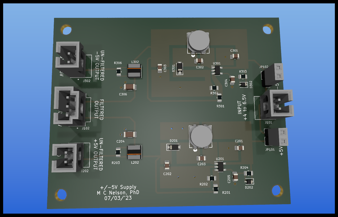
LT193n_+-5V_Supply.png
 
Last edited:
Im using an A0515S isolated dc-dc supply for a project that involves a split rail supply for some op-amps - but have yet to test it.
 
Hi DrM

Looking good. How much current and at what voltage ripple are you getting out of your design?

I have now used a charge pump device to do something similar but with 5V input and +-4V outputs. I have a DAQ board which requires a bipolar supply for some front end op-amps.
https://www.ti.com/general/docs/sup...10&gotoUrl=https://www.ti.com/lit/gpn/lm27762

Very low part count and cost but cannot boost so output must be below the supply level.

Another option I have not used but has fixed +5V and -5V outputs with reasonably low cost and low part count implementation:

https://www.ti.com/lit/ds/symlink/t...tps%3A%2F%2Fwww.ti.com%2Flit%2Fgpn%2Ftps65133
 
@strud The LM27762 is a little different. In that device, the positive supply is generated from an LDO. For a +4V output (from USB in) you are probably okay (the LDO will drop out for voltages near USB).

Even for a 4V design, I think you would be much better off with a +5V supply, for at least two reasons. (a) rail to rail is not really rail to rail and (b) there are few such opamps that also have low current noise suitable for an instrument input (i.e., pA/√Hz) and even fewer with a slew of more than a few V/usec.

(Why do we need pA/√Hz for an instrumentation input? For a 1 megohm source at 100Khz, 1nA/√Hz of current noise becomes 0.1V of voltage noise, and that is at the input).

In a few days, I hope to post two new designs, an instrumentation input and analog output, both 16bit, 1Msps, SPI, and I think, noise < 1 LSB.
 
I want to mention two more details about the dual supply design shown in the original post.

1) The LT1930 is used in the SEPIC configuration. The board provides +5V and -5V, even when the input is well below USB, to as low as 2.6V. And, the LT1930 and LT1931 can each provide better than 300mA each.

2) We looked at some devices that provide dual supplies. We thought about it, did some careful analysis, and as I recall, I think, we ultimately chose to use separate devices for better heat management, more current and the option of using one or the other as you see in the jumpers.
 
Last edited:
Hi DrM

My ADC input full range is only +-1.2V hence the +-4V is plenty of room.

I am using these as my front end buffer amplifiers. They are working very well in my current application.
https://www.ti.com/general/docs/sup...=10&gotoUrl=http://www.ti.com/lit/gpn/ths4561

Your design looks very well thought through, I have different requirements for space and cost.

Very interested to see your high speed analog designs. What application do you have for those?
 
@strud Looks nice, pretty good current noise, slew, CMRR, PSRR. Is the max diff input +/-1V, enough for your application?

Re the designs. I am posting a series of designs and firmware to my github page. Some of these are designs that I have been using in my lab and some are new. Generally the idea is to help remove one of the barriers to doing science, by making professional, even high end, capabilities economically accesible. I especially enjoy that most of the designs have BOMs under $100 and compete well against commercial offerings that come with a few more zeros.

I study organic electronics and in particular, lasing at ultra low current density in organic semiconductors. My lab is run by T3.2s and T4s and Python running on Linux desktops.
 
To avoid EMI problems and to ensure performance, the layout should be way way more compact.
Layout hints are respected, but components around the LT1930 and LT1931 are too much dispersed.

Angelo
 
@Angelo Here are the layouts from the datasheet (and another of the board). You'll notice they look a lot like the board. In fact, originally, I traced one of them. The other has one mod for the septic. And, the design was reviewed by two engineers at Analog.

Nonetheless, I appreciate that the datasheet says little about why the layout has to be this way. Part of it is managing the return path. Note the note about the cut for example. The large areas may also be for heat management. The other side is a ground plane, which you can see more clearly in the third image below. I doubt that it is a good antenna.

We use these with a current amplifier to measure fast pico-ampere phenomena in organic semiconductors. So far they seem pretty quiet.

Screenshot from 2024-01-24 05-40-48.png
Screenshot from 2024-01-24 05-41-52.png


Here is an image of the design where you can see the ground plane

Screenshot from 2023-07-05 13-15-27.p400.jpg
 
@Angelo Thinking about it some more, in the areas that are not directly connected to the IC, maybe I could squeeze it a bit. When you look at it carefully though, I don't think it is going to improve anything very much. But, maybe I'll try it if I find the time.
 
And to filter the current flow, both input and output, current should be forced to go to the capacitor pad, and then continue from the pad to the next connexion.


Angelo
 
@Angelo Again, that is what it does. It is a working design that has been used for years. It was developed in consultation with another very expert instrumentation physicist and the engineers at Analog, and we do understand impedance, one of us taught the course. I appreciate suggestions, but I don't think youre going to find much of any substance to pick at.
 
I don't say it is a bad design. I just say it could be better with some minor modifications.

I made some implementations, which were "perfect" from my point of view. Even after reading a lot of application notes. My collegue made some measurements, and in 5 minutes, my design went from "perfect" to "perfect example for how not to do this".
This was mainly due to bad placement in respect to current flow loops and trace routing from component to another.

Angelo
 
Is this used with Teensy? Perfectly fine to discuss power supplies... but this was posted in the Blog Project Submission section. To show a project on the website blog, it needs to somehow use Teensy.
 
This +/-5V supply is the enabling piece for a lot of the circuits that I build specifically to use with the Teensy.

For example, I am about to spin a new instrumentation interface and a waveform generator, both 16 bits 1MHz to use with the Teensy 4.0. They require the speed of the Teensy 4.0, including its 480MHz USB, and they require +/-5V supplies. There is a current to voltage amplifier input also, and again absolutely requires dual rails.

In general, the Teensy provides some extra capability, and if you want to take advantage of it, you very often need to be able to design circuiits that go beyond single ended supplies. And when the goal is high precision, or super high gain, even moreso, you need a quiet supply.

So this is the enabling piece for those designs.
 
Back
Top