PT8211 with irregular clocking signals (non I2S) from T4

rvh

Well-known member
For some time now I've been trying to find a way to have a continuously variable output sampling rate solution for T4.x to take the place of the ever more precarious T3.6 situation.
While adding a parallel DAC is going to be my last resort, I was wondering if a serial DAC like the PT8211 can be used by 'manually clocking' data from the T4. i.e. rather than set up the I2S interface, use a dedicated bit-toggling routine to send the correct states to three digital output pins (these could still be pins 7,20,21).

The idea would be to call that routine at the time I would normally write to the DAC on a T3.6, and have it send the three "serial signals" at something close to the max rate the PT8211 can handle, and then have them sit idle until the next DAC output is needed.

Is this at all plausible with something like the PT8211 (or alternative suggestions), or will serial DACs like this fall over in a heap because they need a steady clock/data/WS stream?

I looked at the PT8211 data sheet, but it's very concise and the timing diagram is not very helpful. The sheet says the chip allows a wide range of frequencies, and throws away data beyond 16 bits, but I can't see how it determines when the MSB is available.
 
or will serial DACs like this fall over in a heap because they need a steady clock/data/WS stream?
Interesting question. Actually I have no idea. But I can imagine that this could work since the PT8211 is a very basic DAC.
I would not be surprised if there is just an ordinary 16 bit shift-register where the DIN data is clocked-in on BCK [MSB first] and latched on a trailing or falling edge of the WS signal. After latching the 16 bits, these are converted to voltage by the R-2R resistor ladder network.

I assume that you do not have a PT8211 at hand now, otherwise a quick test could bring more clearity.
If you want, I can do some testing for you. Just send me some bit-banging code [I don't have time to write the code myself] and I'll test it.

Paul

Thanks Paul, I too was thinking it might be a simple enough chip for this to work. It would be great if you could do a quick test for me, as indeed I don't have a PT8211 board (they seem not available in Australia, so I will order some from you if it works). I'll try to write some simple code as soon as I can.

I think I read somewhere that some of these DACs need the edge of the WS signal to occur one bit earlier than the first (MSB), so we might need to try a few variations. Also, if running a T4 at 600MHz, what would you suggest the best way would be for me to set the time between clocks/bits so that the PT8211 can handle the rate?

Thanks,
Richard
 
p.s. How would you rate the audio quality (and background noise) you get from the PT8211 board vs a T3.6 DAC, when powered by USB (perhaps with an isolator)?
 
Paul , here's a first go at a test program that sends 100 and 200Hz sawtooth waves to R and L channels respectively.

I'm assuming the rudimentary timing diagram in the PT8211 data sheet is accurate where it shows one clock cycle is executed after a WS edge before data starts to be clocked. I've set the clock rate at half the max allowed. If this happens to work, you could try halving the value of HALFCLKns to 25ns to push it to its max.

I'm assuming also that it's OK to use the result of the & operator in digitalWriteFast to set the pin high for any non-zero result.

Code:
#define DIN 7
#define BCLK 21 // max 20Mhz (50ns), using 2x slower when HALF
#define WS 20
#define HALFCLKns 50    // clock cycle duration rate is twice this 

int16_t saw=0;
int16_t saw2=0;
int16_t m[16] = {0x8000,0x4000,0x2000,0x1000,0x0800,0x4000,0x0200,0x0100,0x0080,0x0040,0x0020,0x0010,0x0008,0x0004,0x0002,0x0001};

elapsedMicros sampletime;  

void setup() 
{
  digitalWrite(DIN,0);
  digitalWrite(BCLK,0);
  digitalWrite(WS,0);
  pinMode(DIN, OUTPUT);  
  pinMode(BCLK, OUTPUT); 
  pinMode(WS, OUTPUT);  
}

void loop() {
 
  
 if(sampletime >= 25)  // 40kHz
 {
   sampletime=0;

   saw += 160;  // 400 steps per cycle = 100Hz
   if(saw >= 32000) 
   {
      saw -= 64000;          
   } 
   saw2 += 320;  // 200 steps = 200Hz
   if(saw2 >= 32000) 
   {
      saw2 -= 64000;
   }  
  
  // at 10MHz (HALFCLKns 50) bit banging takes up 3.4us for delaynanoseconds calls, plus around 100x digitalWriteFast times 
  // total appears to be about 5us 
   
  //--   WS=0, Right  
    digitalWriteFast(BCLK,0); 
    digitalWriteFast(DIN,0);         // probably don't need this
    digitalWriteFast(WS,0);   
    delayNanoseconds(HALFCLKns);
    digitalWriteFast(BCLK,1); 
    delayNanoseconds(HALFCLKns);
    for (int i=15; i>=0; i--)
    {
      digitalWriteFast(BCLK,0); 
      digitalWriteFast(DIN,saw & m[i]); 
      delayNanoseconds(HALFCLKns);
      digitalWriteFast(BCLK,1); 
      delayNanoseconds(HALFCLKns);
    }  
    
  //-- WS=1, LEFT
    digitalWriteFast(BCLK,0);
    digitalWriteFast(DIN,0);         // probably don't need this    
    digitalWriteFast(WS,1);    
    delayNanoseconds(HALFCLKns);
    digitalWriteFast(BCLK,1); 
    delayNanoseconds(HALFCLKns);
    for (int i=15; i>=0; i--)
    {
      digitalWriteFast(BCLK,0); 
      digitalWriteFast(DIN,saw2 & m[i]); 
      delayNanoseconds(HALFCLKns);
      digitalWriteFast(BCLK,1); 
      delayNanoseconds(HALFCLKns);
    } 
 }
}
 
I had another read of the data sheet, and now think any WS edge might terminate the data input sequence for a channel. Even though that seems to contradict the statement that only the 'first 16 bit data is valid' - the timing diagram suggests it retains only the final 16 bits if more than 16 are sent. This would make sense in terms of a simple shift register too, which would stop shifting on the WS edge.

If this is right, the test code above might yet work, but it might be safer to latch the second channel immedaitely after the 16th bit, rather than wait for the next sample cycle. i.e. add three lines at the end like this:
Code:
#define DIN 7
#define BCLK 21 // max 20Mhz (50ns), using 2x slower when HALFCLKns = 50
#define WS 20
#define HALFCLKns 50    // clock cycle duration is twice this 

int16_t saw=0;
int16_t saw2=0;
int16_t m[16] = {0x8000,0x4000,0x2000,0x1000,0x0800,0x4000,0x0200,0x0100,0x0080,0x0040,0x0020,0x0010,0x0008,0x0004,0x0002,0x0001};

elapsedMicros sampletime;  

void setup() 
{
  digitalWrite(DIN,0);
  digitalWrite(BCLK,0);
  digitalWrite(WS,0);
  pinMode(DIN, OUTPUT);  
  pinMode(BCLK, OUTPUT); 
  pinMode(WS, OUTPUT);  
}

void loop() {
 
  
 if(sampletime >= 25)  // 40kHz
 {
   sampletime=0;

   saw += 160;  // 400 steps per cycle = 100Hz
   if(saw >= 32000) 
   {
      saw -= 64000;          
   } 
   saw2 += 320;  // 200 steps = 200Hz
   if(saw2 >= 32000) 
   {
      saw2 -= 64000;
   }  
  
  // at 10MHz (HALFCLKns 50) bit banging takes up 3.4us for delaynanoseconds calls, plus around 100x digitalWriteFast times 
  // total appears to be about 5us 
   
  //--   WS=0, Right  
    digitalWriteFast(BCLK,0); 
    digitalWriteFast(DIN,0);         // probably don't need this
    digitalWriteFast(WS,0);          
    delayNanoseconds(HALFCLKns);
    digitalWriteFast(BCLK,1); 
    delayNanoseconds(HALFCLKns);
    for (int i=15; i>=0; i--)
    {
      digitalWriteFast(BCLK,0); 
      digitalWriteFast(DIN,saw & m[i]); 
      delayNanoseconds(HALFCLKns);
      digitalWriteFast(BCLK,1); 
      delayNanoseconds(HALFCLKns);
    }  
    
  //-- WS=1, LEFT
    digitalWriteFast(BCLK,0);
    digitalWriteFast(DIN,0);         // probably don't need this    
    digitalWriteFast(WS,1);    
    delayNanoseconds(HALFCLKns);
    digitalWriteFast(BCLK,1); 
    delayNanoseconds(HALFCLKns);
    for (int i=15; i>=0; i--)
    {
      digitalWriteFast(BCLK,0); 
      digitalWriteFast(DIN,saw2 & m[i]); 
      delayNanoseconds(HALFCLKns);
      digitalWriteFast(BCLK,1); 
      delayNanoseconds(HALFCLKns);
    } 
    digitalWriteFast(BCLK,0); 
    digitalWriteFast(DIN,0);         // probably don't need this
    digitalWriteFast(WS,0);         
 }
}
 
so I will order some from you if it works
Hi Richard, you're not accidently mixing me up with Paul Stoffregen, founder of PJRC.com, do you? I don't have shop...
Also I don't have a Teensy 3.6 so can't tell you about its DAC quality.

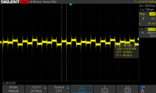
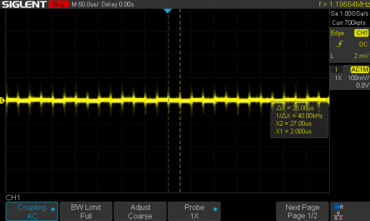
Anyway, I tested your code from msg #5 and this what the scope shows:

code#5.png

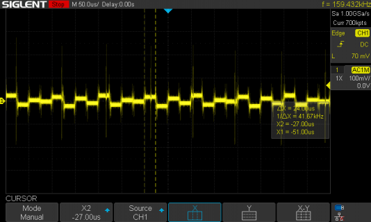
And here is the scope image with your code from msg #6:

code#6.png

Seems identical but not a sawtooth by far.
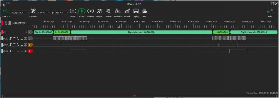
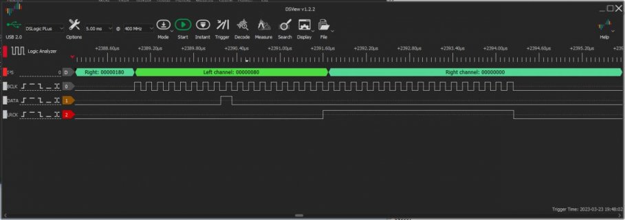
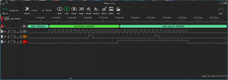
Now I'm going to hook up the logic analyzer and see what the I2S signals look like. I will use the code from msg #6.

Stay tuned,
Paul
 
Hi Richard, you're not accidently mixing me up with Paul Stoffregen, founder of PJRC.com, do you? I don't have shop...
Also I don't have a Teensy 3.6 so can't tell you about its DAC quality.

Anyway, I tested your code from msg #5 and this what the scope shows:

View attachment 30689

And here is the scope image with your code from msg #6:

View attachment 30690

Seems identical but not a sawtooth by far.
Now I'm going to hook up the logic analyzer and see what the I2S signals look like. I will use the code from msg #6.

Stay tuned,
Paul

Thanks Paul, all much appreciated (and sorry about the mix up with the other Paul). I rechecked the code above and realized it's sending the wrong bit order as well as having one value wrong in the 'and' array. So I've corrected that below. You can verify it's sending twos complement data by uncommenting the new lines I added in the setup routine.

But I'll be surprised if it will work because even with the wrong bit order previously, you should have seen large signals at the DAC output, even though it would be noise rather than a saw tooth. Not the very small signal you showed, which seems to indicate the chip's not happy about something else and not actually converting the data.

Code:
#define DIN 7
#define BCLK 21 // max 20Mhz (50ns), using 2x slower when HALFCLKns = 50
#define WS 20
#define HALFCLKns 50    // clock cycle duration is twice this 

int16_t saw=0;
int16_t saw2=0;
int16_t m[16] = {0x8000,0x4000,0x2000,0x1000,0x0800,0x0400,0x0200,0x0100,0x0080,0x0040,0x0020,0x0010,0x0008,0x0004,0x0002,0x0001};

elapsedMicros sampletime;  

void setup() 
{
  digitalWrite(DIN,0);
  digitalWrite(BCLK,0);
  digitalWrite(WS,0);
  pinMode(DIN, OUTPUT);  
  pinMode(BCLK, OUTPUT); 
  pinMode(WS, OUTPUT);  

  //int16_t testval = -16384;
  //for (int i=0; i<16; i++)
  //{
  //    if(testval & m[i]) Serial.print("1");
  //    else Serial.print("0"); 
  //}  
  //Serial.println("");
}

void loop() {
 
  
 if(sampletime >= 25)  // 40kHz
 {
   sampletime=0;

   saw += 160;  // 400 steps per cycle = 100Hz
   if(saw >= 32000) 
   {
      saw -= 64000;          
   } 
   saw2 += 320;  // 200 steps = 200Hz
   if(saw2 >= 32000) 
   {
      saw2 -= 64000;
   }  
  
  // at 10MHz (HALFCLKns 50) bit banging takes up 3.4us for delaynanoseconds calls, plus around 100x digitalWriteFast times 
  // total appears to be about 5us 
   
  //--   WS=0, Right  
    digitalWriteFast(BCLK,0); 
    digitalWriteFast(DIN,0);         // probably don't need this
    digitalWriteFast(WS,0);          
    delayNanoseconds(HALFCLKns);
    digitalWriteFast(BCLK,1); 
    delayNanoseconds(HALFCLKns);
    for (int i=0; i<16; i++)
    {
      digitalWriteFast(BCLK,0); 
      digitalWriteFast(DIN,saw & m[i]); 
      delayNanoseconds(HALFCLKns);
      digitalWriteFast(BCLK,1); 
      delayNanoseconds(HALFCLKns);
    }  
    
  //-- WS=1, LEFT
    digitalWriteFast(BCLK,0);
    digitalWriteFast(DIN,0);         // probably don't need this    
    digitalWriteFast(WS,1);    
    delayNanoseconds(HALFCLKns);
    digitalWriteFast(BCLK,1); 
    delayNanoseconds(HALFCLKns);
    for (int i=0; i<16; i++)
    {
      digitalWriteFast(BCLK,0); 
      digitalWriteFast(DIN,saw2 & m[i]); 
      delayNanoseconds(HALFCLKns);
      digitalWriteFast(BCLK,1); 
      delayNanoseconds(HALFCLKns);
    } 
    digitalWriteFast(BCLK,0); 
    digitalWriteFast(DIN,0);         // probably don't need this
    digitalWriteFast(WS,0);         
 }
}


In the data sheet it says "the buffered DIN data then feeding to the DAC after both input register are all settled down, this can eliminated the phase shift happened between two channel output." But I'm not sure what determines that condition. Maybe there are subsequent clock cycles needed after (one of?) the WS edges to synchronously transfer L+R data to the DACs. But there's not enough info.
 
Last edited:
But I'll be surprised if it will work because even with the wrong bit order previously, you should have seen large signals at the DAC output, even though it would be noise rather than a saw tooth

I realized later that the reverse bit order might actually be enough to cause the result you showed due to the fact that the saw wav is incremented in steps of 160. Normally that would cause the lowest 5 bits to always remain at 0, but in reverse order it would cause the 5 most significant bits to be 0, which would produce a fairly small signal (maybe 80mV max).
 
Thanks agian Paul. I dusted off my oscilloscope to check the signals I was generating with that code, and discovered the DIN streams were still not setting higher bits. There must be a problem with my use of saw & m in the digital write command. Sorry about that. I've replaced it in the following code with a right shift of the saw values followed by &1. On my oscilloscope the data now look like they're spanning the correct range. Hopefully this will produce saw waves at the PT8211 output.

Code:
#define DIN 7
#define BCLK 21 // max 20Mhz (50ns), using 2x slower when HALFCLKns = 50
#define WS 20
#define HALFCLKns 50    // clock cycle duration is twice this 
int16_t saw=0;
int16_t saw2=0;
elapsedMicros sampletime;  

void setup() 
{
  digitalWrite(DIN,0);
  digitalWrite(BCLK,0);
  digitalWrite(WS,0);
  pinMode(DIN, OUTPUT);  
  pinMode(BCLK, OUTPUT); 
  pinMode(WS, OUTPUT);  
}

void loop() {
 if(sampletime >= 25)     // 40kHz
 {
   sampletime=0;
   saw += 160;            // 400 steps per cycle = 100Hz
   if(saw >= 32000)    
      saw -= 64000;             
   saw2 += 320;           // 200 steps = 200Hz
   if(saw2 >= 32000)    
      saw2 -= 64000;    
  
  // at 10MHz (HALFCLKns 50) bit banging takes up 3.4us for delaynanoseconds calls, plus around 100x digitalWriteFast times 
  // total appears to be about 5us 
   
  //--   WS=0, Right  
    digitalWriteFast(BCLK,0); 
    digitalWriteFast(DIN,0);         // probably don't need this
    digitalWriteFast(WS,0);          
    delayNanoseconds(HALFCLKns);
    digitalWriteFast(BCLK,1); 
    delayNanoseconds(HALFCLKns);
    for (int i=15; i>=0; i--)
    {
      digitalWriteFast(BCLK,0); 
      digitalWriteFast(DIN, (saw>>i) & 1); 
      delayNanoseconds(HALFCLKns);
      digitalWriteFast(BCLK,1); 
      delayNanoseconds(HALFCLKns);
    }  
    
  //-- WS=1, LEFT
    digitalWriteFast(BCLK,0);
    digitalWriteFast(DIN,0);         // probably don't need this    
    digitalWriteFast(WS,1);    
    delayNanoseconds(HALFCLKns);
    digitalWriteFast(BCLK,1); 
    delayNanoseconds(HALFCLKns);
    for (int i=15; i>=0; i--)
    {
      digitalWriteFast(BCLK,0); 
      digitalWriteFast(DIN, (saw2>>i) & 1); 
      delayNanoseconds(HALFCLKns);
      digitalWriteFast(BCLK,1); 
      delayNanoseconds(HALFCLKns);
    } 
    digitalWriteFast(BCLK,0); 
    digitalWriteFast(DIN,0);         // probably don't need this
    digitalWriteFast(WS,0);         
 }
}
 
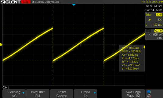
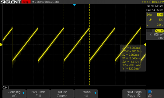
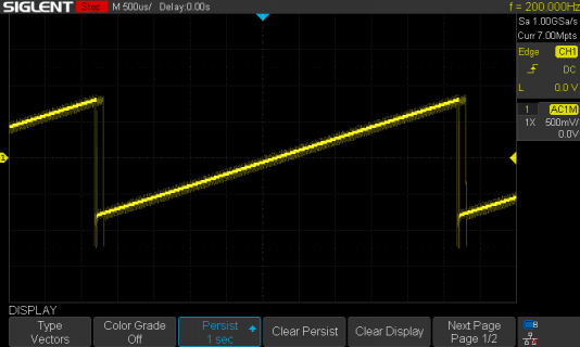
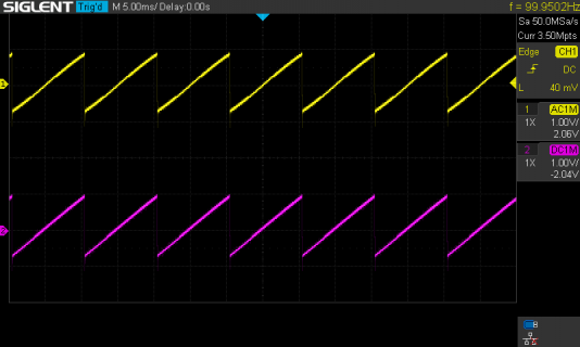
There are your sawtooths:
Paul

Fabulous! Thanks very much. Looks like this approach should solve my problem and allow me to migrate my T3.6 project (that needs variable DAC write times) to T4.1. Are you using the PJRC PT8211 board here? If so, do you find it has much noise feeding into the audio? It looks fairly clean in your pics, but I noticed that board it has just some DC blocking capacitors and no post LPF as recommended in the PT8211 data sheet for better noise performance.
 
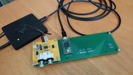
Are you using the PJRC PT8211 board here?
Yep, shown here:

IMG_20230325_111002.jpg

Yeah it's a bit noisy, the scope trigger was hardly able to show a stable image. Here is a screenshot of the scope with a 1sec persistence:

SDS00087.png

You may want to check out this thread where I did some measurements on different audio boards including the PT8211.

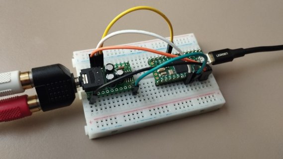
By the way, the logic analyzer was hooked up to a different T4 board assembly because it has long header pins for easy connecting the LA leads.
As you can see below, there is another audioboard [DAC PCM5102A based]. That I2S DAC does not show the sawtooths with your latest code - not exactly surprised here.

IMG_20230325_092430.jpg

Paul
 
Yep, shown here:
You may want to check out this thread where I did some measurements on different audio boards including the PT8211.


One forum member in the other thread you mention was very negative about the PT8211, saying it was worse than the T4 "medium-quality-audio" output. Is that to your knowledge the general consensus these days? If so, I should check out the medium-quality-audio option, which I had dismissed outright without trying it.

For my current application, I just need the quality to be no worse than the DAC output of a T3.6 (up to about 40-50kHz). So if anyone has compared the T3.6 and the PT8211 for audio quality, I'd love to hear your impressions.
 
Last edited:
Both PT8211 and MQS sound pretty good to my ears. If you have a 1K resistor and 0.01uF capacitor handy, give MQS a quick try. I believe you may be surprised how good it sounds.

MQS uses a noise shaping algorithm, so it can only work reliably if you keep a consistent sample rate. It really isn't adaptable to non-audio usage where you update the DAC with irregular timing.

If you connect with only a resistor and capacitor, MQS is has no PSRR (power supply rejection ratio), or perhaps 3dB if you consider the PWM is low 50% of the time, but not what you'd expect from a real DAC. It's the same situation as with any other PWM low pass filtered. If your 3.3V power has audio bandwidth noise, it ends up mixed into your audio signal, because it's on the logic level high portion of the PWM. Of course you can create a "clean" power rail and run a buffer chip from it. But if you're going to add an inexpensive buffer chip, PT8211 is so cheap that you're probably better off using it. Then again, how well PT8211 rejects noise from its 3.3V power is an open question. Normally it's used with a resistor and large capacitor to try to clean up the 3.3V power. With either, if you're going to run other circuitry from the 3.3V power, make sure you test your audio quality in the presence of other hardware making the 3.3V power "dirty".

It's easy to obsess too much about audio specs. None of these are considered high quality. PT8211, MQS, or built in 12 bit DACs aren't going to win any audiophile awards! But they all can sound pretty good. When you just need something which sounds decent, real listening tests are pretty important.
 
Thanks for the MQS details Paul. Unfortunately if it's not well suited to variable sampling times it's not going to work for me anyway. So I'll try the PT8211, possibly with a LPF after its output. I'm not looking for audiophile performance in this application. The 12 bit DAC quality of the T3.6 works fine (and presumably it has no LPF?), so I just need the PT8211 to match that. Totally agree that a listening test is the way to decide if the quality is sufficient.
 
Many thanks for all the tests and the idea in general. For me these tests indicate that the PT8211 with it's ability of asynchronous communication (no need for a steady data stream) will be perfectly suited as a cheap 16 Bit R2R DAC (actually two in one package) for Control Voltage generation in a DIY polyphonic synth project (with VCOs, VCAs and analog filter chips) where a Teensy 4 will only be used for MIDI processing and modulation generation (LFOs, ADSRs etc.). The PT8211 should easily be able to generate relatively slow changing DC-coupled signals. Maybe its linearity won't be good enough for the VCO frequency CV, but almost certainly for everything else. It will still be a big cost saving factor even if i need better DACs only for the VCO frequency.

For an 8-voice (2 VCOs per voice) synth i will need at least 32 PT8211 (64 CV channels). I will probably program a very low cost FPGA (LCMXO2-1200HC) to do the correct multiplexing for all these PT8211, so that i can drive them easily with simple SPI FIFO burst write commands from the Teensy (no blocking write conditions)

Well, we'll see how it goes.
 
Just an update for anyone else looking to replace the T3.6 with its onboard DAC by using T4.x and the PT8211, especially for projects that require asynchronous data writes.

By using the bit banging method described in this thread with a T4.1 and PT8211, followed by the LPF circuit recommended in the PT8211 data sheets, the audio quality I get is at least as good, and very likely better than what I was getting with the T3.6. Depending on your application, the LPF may not be necessary. But if you are looking for the best quality you can get with this setup, and are powering it via USB, a USB isolator is a must (as with the T3.6).

Finally I'm able to migrate to T4.1, and can stop running T3.6 boards at 256MHz (when you can get them)!
 
Last edited:
I figured out that if you write only to the left channel, then the same signal comes out of both channels. If HALFCLKns is set to the lowest possible value 28, both output channels can be updated in about 1us:
Code:
  digitalWriteFast(WS,1);           // write to left channel
  for (int i=15; i>=0; i--)
  {
    digitalWriteFast(DIN, (value>>i) & 1); 
    delayNanoseconds(HALFCLKns);
    digitalWriteFast(BCLK,1); 
    delayNanoseconds(HALFCLKns);
    digitalWriteFast(BCLK,0); 
  } 
  digitalWriteFast(WS,0);           // both analog outputs are updated
 
That's weird. Would you mind posting your complete code (don't know what "value" is) that shows this behaviour so that I can hook up the logic analyzer and check the data?

Thanks,
Paul
 
I did only rename "saw" to "value". The pin definitions and setup are the same as in your code. Some unnecessary lines removed.
 
Can confirm the observation by mkoch.
Here is the scope image:

SDS00090.png

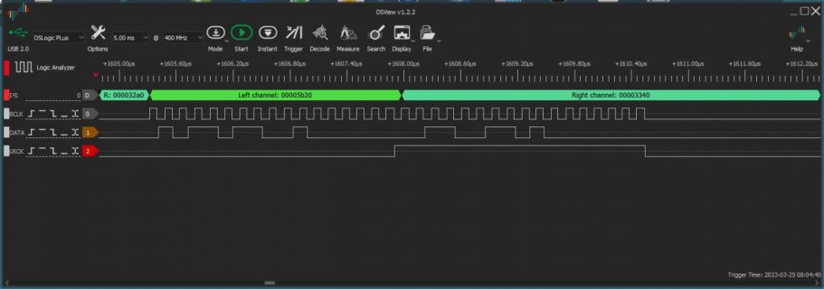
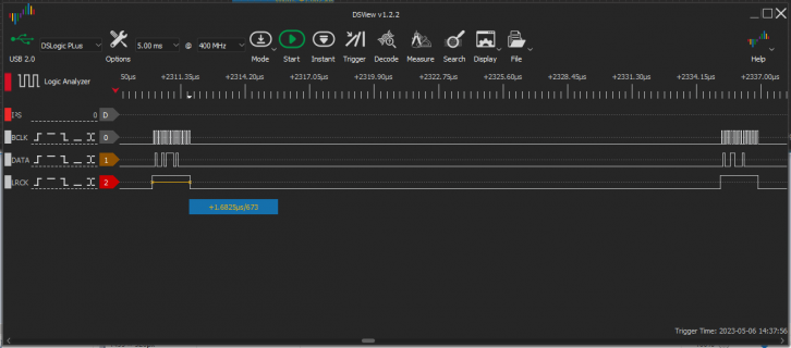
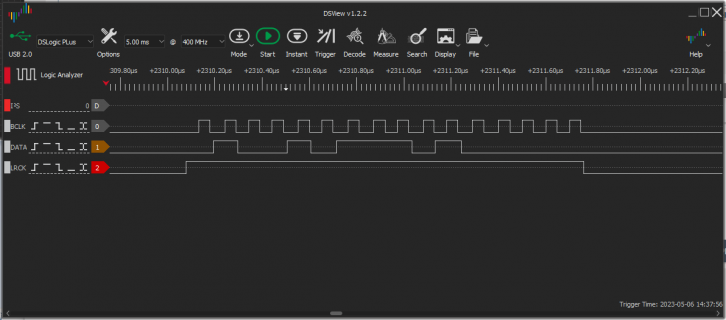
And here is what the logic analyzer shows:

LA_1.68us.png LA_detail.png

For completeness, here is the code that shows the behaviour:
Code:
// https://forum.pjrc.com/threads/72446-PT8211-with-irregular-clocking-signals-(non-I2S)-from-T4
// code from msg#12 & msg#22

#define DIN 7
#define BCLK 21 // max 20Mhz (50ns), using 2x slower when HALFCLKns = 50
#define WS 20
#define HALFCLKns 28    // clock cycle duration is twice this 
int16_t saw = 0;
int16_t saw2 = 0;
elapsedMicros sampletime;

void setup()
{
  digitalWrite(DIN, 0);
  digitalWrite(BCLK, 0);
  digitalWrite(WS, 0);
  pinMode(DIN, OUTPUT);
  pinMode(BCLK, OUTPUT);
  pinMode(WS, OUTPUT);
}

void loop() {
  if (sampletime >= 25)    // 40kHz
  {
    sampletime = 0;
    saw += 160;            // 400 steps per cycle = 100Hz
    if (saw >= 32000)
      saw -= 64000;
    saw2 += 320;           // 200 steps = 200Hz
    if (saw2 >= 32000)
      saw2 -= 64000;
    
    digitalWriteFast(WS, 1);          // write to left channel
    for (int i = 15; i >= 0; i--)
    {
      digitalWriteFast(DIN, (saw >> i) & 1);
      delayNanoseconds(HALFCLKns);
      digitalWriteFast(BCLK, 1);
      delayNanoseconds(HALFCLKns);
      digitalWriteFast(BCLK, 0);
    }
    digitalWriteFast(WS, 0);          // both analog outputs are updated
  }
}

I suppose the internal logic of the PT8211 DAC copies the left channel data to the right channel when no BLCK's have appeared while WS was low and switched to high. Interesting 'feature'...

Paul
 
Back
Top