Reading from OV7670 using FlexIO

KurtE

Senior Member+
As @mjs513 mentioned in another thread, we have been playing around with the OV7670 camera using FlexIO, preferably with DMA
We have had it working on T4.1 using CSI and Micromod using DMA from GPIO pins, but thought it would be fun to get it working properly using
DMA and FlexIO.

We are using the Micromod pins. I had it sort of working with Flexio using just one Shifter, but some of the data was being corrupted. and noticed that the RM for FlexIO Camera example is using 4 shifters and another version we saw was setup to use all 8... So currently trying to use all 8.
Currently with the 4 and 8 setup a read from the camera, dies with either timeout or DMA Error.

Short version question: Has anyone tried FlexIO where you are chaining shift registers to each other so for example with:
4 of them we have 128 bits of data and likewise all 8 256 bits.

If so how have you used DMA to read in the data from the SHIFTBUF[0-7] to be stored out for memory... (Or likewise for something like a display be able to load up all of the Shift buffer registers. with DMA?

Note: the NXP Shifter option has code to configure DMA like:
Code:
/* Configure DMA TCD */
    DMA0->TCD[FLEXIO_CAMERA_DMA_CHN].SADDR = FLEXIO_CAMERA_GetRxBufferAddress(&s_FlexioCameraDevice);
    DMA0->TCD[FLEXIO_CAMERA_DMA_CHN].SOFF = 0u;
    DMA0->TCD[FLEXIO_CAMERA_DMA_CHN].ATTR = DMA_ATTR_SMOD(0u) |
                                            DMA_ATTR_SSIZE(5u) |
                                            DMA_ATTR_DMOD(0u) |
                                            DMA_ATTR_DSIZE(5u);
    DMA0->TCD[FLEXIO_CAMERA_DMA_CHN].NBYTES_MLNO = 32u;
    DMA0->TCD[FLEXIO_CAMERA_DMA_CHN].SLAST = 0u;
    DMA0->TCD[FLEXIO_CAMERA_DMA_CHN].DADDR = (uint32_t)(*pFlexioCameraFrameBuffer);
    DMA0->TCD[FLEXIO_CAMERA_DMA_CHN].DOFF = 32u;
    DMA0->TCD[FLEXIO_CAMERA_DMA_CHN].CITER_ELINKNO = (OV7670_FRAME_BYTES / 32u);
    DMA0->TCD[FLEXIO_CAMERA_DMA_CHN].DLAST_SGA = 0;
    DMA0->TCD[FLEXIO_CAMERA_DMA_CHN].CSR = 0u;
    DMA0->TCD[FLEXIO_CAMERA_DMA_CHN].CSR |= DMA_CSR_DREQ_MASK;
    DMA0->TCD[FLEXIO_CAMERA_DMA_CHN].BITER_ELINKNO = (OV7670_FRAME_BYTES / 32u);

    /* Configure DMA MUX Source */
    DMAMUX->CHCFG[FLEXIO_CAMERA_DMA_CHN] = DMAMUX->CHCFG[FLEXIO_CAMERA_DMA_CHN] &
                                            (~DMAMUX_CHCFG_SOURCE_MASK) |
                                            DMAMUX_CHCFG_SOURCE(FLEXIO_CAMERA_DMA_MUX_SRC);
    /* Enable DMA channel. */
    DMAMUX->CHCFG[FLEXIO_CAMERA_DMA_CHN] |= DMAMUX_CHCFG_ENBL_MASK;
}
Their 4 shifter version was similar:
Code:
static void configDMA(void)
{
    uint32_t soff, smod = 0u, size=0u;

    while(1u << size < DMA_TRSF_SIZE) /* size = log2(DMA_TRSF_SIZE) */
    {
        size++;
    }

    if(DMA_TRSF_SIZE == DMA_MINOR_LOOP_SIZE)
    {
        soff = 0u;
    }
    else
    {
        soff = DMA_TRSF_SIZE;
        while(1u << smod < DMA_MINOR_LOOP_SIZE) /* smod = log2(DMA_MINOR_LOOP_SIZE) */
        {
            smod++;
        }
    }
    
    /* Configure DMA TCD */
    DMA0->TCD[FLEXIO_CAMERA_DMA_CHN].SADDR = FLEXIO_CAMERA_GetRxBufferAddress(&s_FlexioCameraDevice);
    DMA0->TCD[FLEXIO_CAMERA_DMA_CHN].SOFF = soff;
    DMA0->TCD[FLEXIO_CAMERA_DMA_CHN].ATTR = DMA_ATTR_SMOD(smod) |
                                            DMA_ATTR_SSIZE(size) |
                                            DMA_ATTR_DMOD(0u) |
                                            DMA_ATTR_DSIZE(size);
    DMA0->TCD[FLEXIO_CAMERA_DMA_CHN].NBYTES_MLNO = DMA_MINOR_LOOP_SIZE;
    DMA0->TCD[FLEXIO_CAMERA_DMA_CHN].SLAST = 0u;
    DMA0->TCD[FLEXIO_CAMERA_DMA_CHN].DADDR = (uint32_t)(*pFlexioCameraFrameBuffer);
    DMA0->TCD[FLEXIO_CAMERA_DMA_CHN].DOFF = DMA_TRSF_SIZE;
    DMA0->TCD[FLEXIO_CAMERA_DMA_CHN].CITER_ELINKNO = DMA_MAJOR_LOOP_SIZE;
    DMA0->TCD[FLEXIO_CAMERA_DMA_CHN].DLAST_SGA = -OV7670_FRAME_BYTES;
    DMA0->TCD[FLEXIO_CAMERA_DMA_CHN].CSR = 0u;
    DMA0->TCD[FLEXIO_CAMERA_DMA_CHN].CSR |= DMA_CSR_DREQ_MASK;
    DMA0->TCD[FLEXIO_CAMERA_DMA_CHN].BITER_ELINKNO = DMA_MAJOR_LOOP_SIZE;

    /* Configure DMA MUX Source */
    DMAMUX->CHCFG[FLEXIO_CAMERA_DMA_CHN] = DMAMUX->CHCFG[FLEXIO_CAMERA_DMA_CHN] &
                                            (~DMAMUX_CHCFG_SOURCE_MASK) |
                                            DMAMUX_CHCFG_SOURCE(FLEXIO_CAMERA_DMA_MUX_SRC);
    /* Enable DMA channel. */
    DMAMUX->CHCFG[FLEXIO_CAMERA_DMA_CHN] |= DMAMUX_CHCFG_ENBL_MASK;
}

With the 4 one I think it is setup to have inner DMA loop that cycled over the 4 buffers, and then used the Source Mask and the like,
to have the registers work like a circular buffer, so after it reads all 4 (or 8) it recycles back to the first one.

Has anyone tried something like this?

=====
Longer version: More to be filled in tomorrow...


It sort of follows the information within the RM
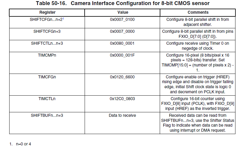

1706580564080.png


The code was more or less a conversion of the 1050 NXP example code.
IO pins:
Code:
#ifdef ARDUINO_TEENSY_MICROMOD
/*
HM01B0 pin      pin#    NXP     Usage
----------      ----    ---     -----
FVLD/VSYNC      33      EMC_07  GPIO
LVLD/HSYNC      32      B0_12   FlexIO2:12
MCLK            7       B1_01   PWM
PCLK            8       B1_00   FlexIO2:16
D0              40      B0_04   FlexIO2:4
D1              41      B0_05   FlexIO2:5
D2              42      B0_06   FlexIO2:6
D3              43      B0_07   FlexIO2:7
D4              44      B0_08   FlexIO2:8  - probably not needed, use 4 bit mode
D5              45      B0_09   FlexIO2:9  - probably not needed, use 4 bit mode
D6              6       B0_10   FlexIO2:10 - probably not needed, use 4 bit mode
D7              9       B0_11   FlexIO2:11 - probably not needed, use 4 bit mode
TRIG            5       EMC_08  ???
INT             29      EMC_31  ???
SCL             19      AD_B1_0 I2C
SDA             18      AD_B1_1 I2C
*/


#define OV7670_PLK   8    //8       B1_00   FlexIO2:16
#define OV7670_XCLK  7    //7       B1_01   PWM
#define OV7670_HREF  46   //32      B0_12   FlexIO2:12
#define OV7670_VSYNC 21   //33      EMC_07  GPIO
#define OV7670_RST   255  // reset pin


#define OV7670_D0    40   //40      B0_04   FlexIO2:4
#define OV7670_D1    41   //41      B0_05   FlexIO2:5
#define OV7670_D2    42   //42      B0_06   FlexIO2:6
#define OV7670_D3    43   //43      B0_07   FlexIO2:7
#define OV7670_D4    44   //44      B0_08   FlexIO2:8  - probably not needed, use 4 bit mode
#define OV7670_D5    45   //45      B0_09   FlexIO2:9  - probably not needed, use 4 bit mode
#define OV7670_D6    6    //6       B0_10   FlexIO2:10 - probably not needed, use 4 bit mode
#define OV7670_D7    9    //9       B0_11   FlexIO2:11 - probably not needed, use 4 bit mode

The flexIO is setup to hopefully chain all 8 Shift buffers to each other: The settings for the FlexIO registers:

At startup the FlexIO registers are:
Code:
FlexIO Configure
 CCM_CSCMR2 = 13192F06
 div1 = 2, div2 = 2
 FlexIO2 Frequency = 120.00 MHz
 CCM_CCGR3 = F00FF333
 FLEXIO2_CTRL = 00000000
 FlexIO2 Config, param=02200808
8Bit FlexIO
 FLEXIO:1 Shifter:0 Timer:0
     SHIFTCFG =  00070100 00070100 00070100 00070100 00070100 00070100 00070100 00070000
     SHIFTCTL =  00000401 00000401 00000401 00000401 00000401 00000401 00000401 00000401
     TIMCMP = 0000003F
     TIMCFG = 01206600
     TIMCTL = 00000401
I2C Write: reg: 0x11(CLKRC), value = 0x0f
I2C Write: reg: 0x6b(DBLV), value = 0x4a
Camera settings:
    width = 320
    height = 240
    bits per pixel = 16
In this run I had a DMA Timeout
Code:
Reading frame
Buffer: 0x20017d2c halfway: 0x2002a92c end:0x2003d52c

DMA CR: 00000482 Channel: 1 80000041
CH: 2000449c 400e9020: SA:401b0200 SO:0 AT:505 (SM:0 SS:5 DM:0 DS:5) NB:20 SL:0 DA:20017d2c DO: 32 CI:12c0 DL:-153600 CS:a BI:12c0
Flexio DMA: length: 153600
Timeout waiting for DMA
 SHIFTSTAT bit was set (000000FF)
 DMA channel #1
 DMAMUX = 80000041
 FLEXIO2_SHIFTSDEN = 01
 TCD CITER = 4800
 TCD CSR = 0000000A
CM: 2000449c 400e9020: SA:401b0200 SO:0 AT:505 (SM:0 SS:5 DM:0 DS:5) NB:20 SL:0 DA:20017d2c DO: 32 CI:12c0 DL:-153600 CS:a BI:12c0
Finished reading frame
I know that the Camera is generating data and that we are seeing some of it. For example in the below Logic Analyzer capture, the last line is where we detect the start of a new frame and the start to capture data.
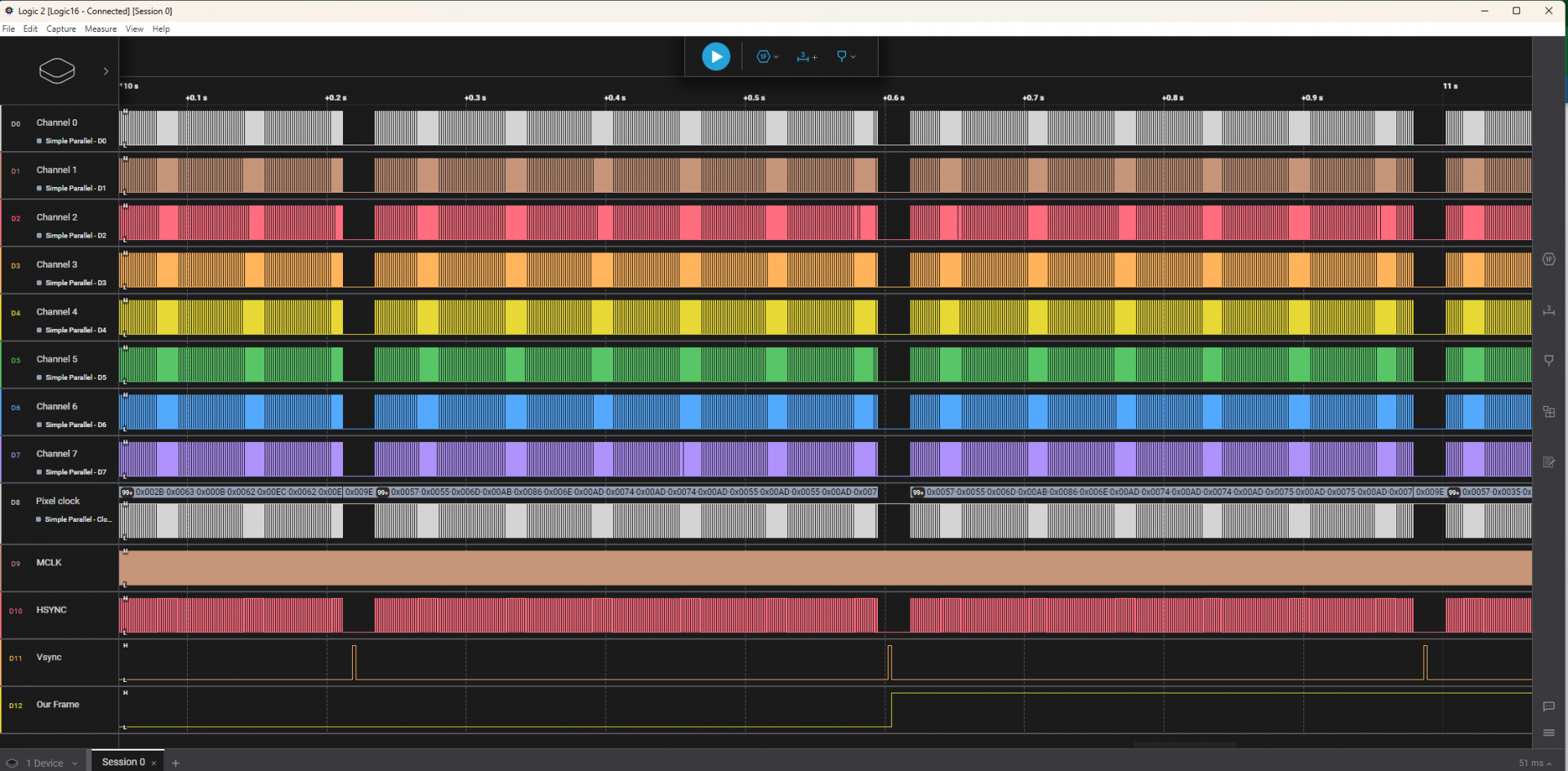
1706581345813.png


More tomorrow after I reread some of the sections again on how the chaining works in FlexIO and likewise:
inner and outer loops.

But suggestions would be appreciated!
 
IIRC you can't chain all eight because they're split into two groups of four (shifter4 can't feed shifter3). I can't recall where I saw this but it was hidden away somewhere - maybe it was a misconception due to the 1050 only having 4 shift buffers, or maybe I'm thinking of the timer registers instead, e.g. timer4 can't enable/disable itself based on timer3.

I use DMA to write to SHIFTBUF0-SHIFTBUF3 in the vga output sample, it's pretty simple; DOFF = 4 (increment by 4 after each write), DMOD = 4 (wrap after 2^4 bytes), DSIZE = 2 (each write is 4 bytes), NBYTES = 16 (minor loop size is 16 bytes).

From the code you posted above it's not clear if SSIZE is always being set to 2 (4 bytes) as it should - the FlexIO shift buffers are 32-bit hardware registers so you can't read from them using any other size.
 
Last edited:
Looks odd to me... again they're setting SSIZE to 5, which does 4x64-bit reads (32 bytes total)... which won't work when the shift buffer hardware registers are only 32-bits wide. It's not safe to access hardware registers with any width other than what they're physically defined with.
 
Looks odd to me... again they're setting SSIZE to 5, which does 4x64-bit reads (32 bytes total)... which won't work when the shift buffer hardware registers are only 32-bits wide. It's not safe to access hardware registers with any width other than what they're physically defined with.
That is some of the stuff that is confusing me as well.
1706621918516.png

I have not seen anywhere that talks about the burst mode... Except that pdf I linked to above:

The code above shows the DMA TCD configurations:• Source address: FlexIO SHIFTBUF0 address.• Source address offset: 0, which means no offset.• Source address modulo: 0, which means that the source address modulo is disabled.• Source data transfer size for each time access: 5, which means 32 bytes burst.• Destination address modulo: 0, which means that the destination address modulo is disabled.• Destination data transfer size for each time access: 5, which means 32 bytes burst.• Minor loop byte count: 32 bytes.• Source minor loop offset mapping: Disabled.• Destination minor loop offset mapping: Disabled.• Last source address adjustment: 0, which means no adjustment.• Destination address: RAM buffer address.• Destination address offset: 0, which means no offset.• Major loop counter: (OV7670_FRAME_BYTES / 32u) = (160 x 120 x 2) / 32 = 1200.• Last destination address adjustment: 0, which means no adjustment. The new destination address is configured in theVSYNC ISR.• Disable the DMA request after each major loop. The request is enabled in the VSYNC ISR each time.

As I mentioned in first post, The 1052 example code has
Code:
/*******************************************************************************
 * Definitions
 ******************************************************************************/
#define FXIO_SHFT_COUNT         4u          /* 4 shifters */
#define DMA_TRSF_SIZE           8u          /* 8 bytes */
#define DMA_MINOR_LOOP_SIZE     16u         /* 16 bytes */
#define DMA_MAJOR_LOOP_SIZE     (OV7670_FRAME_BYTES / DMA_MINOR_LOOP_SIZE)
...
static void configDMA(void)
{
    uint32_t soff, smod = 0u, size=0u;

    while(1u << size < DMA_TRSF_SIZE) /* size = log2(DMA_TRSF_SIZE) */
    {
        size++;
    }

    if(DMA_TRSF_SIZE == DMA_MINOR_LOOP_SIZE)
    {
        soff = 0u;
    }
    else
    {
        soff = DMA_TRSF_SIZE;
        while(1u << smod < DMA_MINOR_LOOP_SIZE) /* smod = log2(DMA_MINOR_LOOP_SIZE) */
        {
            smod++;
        }
    }
    
    /* Configure DMA TCD */
    DMA0->TCD[FLEXIO_CAMERA_DMA_CHN].SADDR = FLEXIO_CAMERA_GetRxBufferAddress(&s_FlexioCameraDevice);
    DMA0->TCD[FLEXIO_CAMERA_DMA_CHN].SOFF = soff;
    DMA0->TCD[FLEXIO_CAMERA_DMA_CHN].ATTR = DMA_ATTR_SMOD(smod) |
                                            DMA_ATTR_SSIZE(size) |
                                            DMA_ATTR_DMOD(0u) |
                                            DMA_ATTR_DSIZE(size);
    DMA0->TCD[FLEXIO_CAMERA_DMA_CHN].NBYTES_MLNO = DMA_MINOR_LOOP_SIZE;
    DMA0->TCD[FLEXIO_CAMERA_DMA_CHN].SLAST = 0u;
    DMA0->TCD[FLEXIO_CAMERA_DMA_CHN].DADDR = (uint32_t)(*pFlexioCameraFrameBuffer);
    DMA0->TCD[FLEXIO_CAMERA_DMA_CHN].DOFF = DMA_TRSF_SIZE;
    DMA0->TCD[FLEXIO_CAMERA_DMA_CHN].CITER_ELINKNO = DMA_MAJOR_LOOP_SIZE;
    DMA0->TCD[FLEXIO_CAMERA_DMA_CHN].DLAST_SGA = -OV7670_FRAME_BYTES;
    DMA0->TCD[FLEXIO_CAMERA_DMA_CHN].CSR = 0u;
    DMA0->TCD[FLEXIO_CAMERA_DMA_CHN].CSR |= DMA_CSR_DREQ_MASK;
    DMA0->TCD[FLEXIO_CAMERA_DMA_CHN].BITER_ELINKNO = DMA_MAJOR_LOOP_SIZE;

    /* Configure DMA MUX Source */
    DMAMUX->CHCFG[FLEXIO_CAMERA_DMA_CHN] = DMAMUX->CHCFG[FLEXIO_CAMERA_DMA_CHN] &
                                            (~DMAMUX_CHCFG_SOURCE_MASK) |
                                            DMAMUX_CHCFG_SOURCE(FLEXIO_CAMERA_DMA_MUX_SRC);
    /* Enable DMA channel. */
    DMAMUX->CHCFG[FLEXIO_CAMERA_DMA_CHN] |= DMAMUX_CHCFG_ENBL_MASK;
}

so if I am computing correctly:
with DMA_TRSF_SIZE=8 size=3 (64 bit) used for SSIZE and DSIZE
SMOD with DMA_MINOR_LOOP_SIZE = 16, smod=4
and SOFF = DMA_TRSF_SIZE = 8

I am wondering in both cases, if the system still reads and writes 32 bits at a time, and then internally increments to the next logical address, and in the case of the FLEXIO Shift buffers we have:
Code:
volatile uint32_t SHIFTBUF[8];          // 0x200 204 208 20c (IMXRT_FLEXIO1.offset200)
So it increments logically through each of the 8 shift buffers...

But I don't have any good comfortable feelings about this...
They probably did it differently between these two sources as if they wanted to transfer the 128 bits (16 bytes), they might have wanted to configure for this but this is not a valid SSIZE or DSIZE...
 
I guess the easy way to check would be to put something in shifter buffers and then try to read it as 8 bytes:
Code:
FLEXIO2_SHIFTBUF0 = 0x89ABCDEF;
FLEXIO2_SHIFTBUF1 = 0x01234567;
uint64_t i = *(uint64_t*)&FLEXIO2_SHIFTBUF0;
printf("Result: %llx\n", i);
since that will be the same as how the DMA engine is accessing them when programmed with SSIZE=3 or 5.
Thanks,
It appears to work.

Code:
void setup() {
  // put your setup code here, to run once:
  while (!Serial) {}
  Serial.begin(115200);
  CCM_CCGR3 |= CCM_CCGR3_FLEXIO2(CCM_CCGR_ON);
  FLEXIO2_SHIFTBUF0 = 0x89ABCDEF;
  FLEXIO2_SHIFTBUF1 = 0x01234567;
  uint64_t i = *(uint64_t*)&FLEXIO2_SHIFTBUF0;
  Serial.printf("Result: %llx\n", i);
}
void loop() {
}

Code:
Result: 123456789abcdef
 
💡 - Getting closer... The DMA Error was because the output buffer was not 64 bit (maybe only 32 bit) aligned... It as setup for 16 bit pixels.
So once I aligned it... In this case to 32 byte alignment... it started receiving data.

I may still have a few alignment issues with this. In that I am showing garbage.
But again hints: We print out the starting pixels for some lines and I see:
Code:
DMA CR: 00000482 Channel: 1 80000001
CH: 20029c9c 400e9020: SA:401b0200 SO:0 AT:505 (SM:0 SS:5 DM:0 DS:5) NB:20 SL:0 DA:20004000 DO: 32 CI:12c0 DL:-153600 CS:a BI:12c0
Flexio DMA: length: 153600
CM: 20029c9c 400e9020: SA:401b0200 SO:0 AT:505 (SM:0 SS:5 DM:0 DS:5) NB:20 SL:0 DA:20004000 DO: 32 CI:12c0 DL:-153600 CS:8a BI:12c0
Finished reading frame

20004000: 6700 1296 90bd 90bd 90bd 90bd b0bd b0bd ....41e9 3ae9 4209 2909 3906 31a8 3148 3969
20004280: 0000 0000 0000 0000 0000 0000 0000 0000 ....4a2a 4a8c 528c 52ac 42ac 392a 3968 4267
20004500: 4a00 424b 426b 428b 3a6c 422a 424b 4a4b ....4188 4a88 412b 49ea 41ca 49ca 41ea 39c9
20004780: 5200 410a 49a9 4aea 524b 524c 52ac 4a8c ....494a 294a 4a52 494a 6a52 0842 6631 e941

Show Center pixels
1706648022058.png
 
Thanks,
It appears to work.
Actually, I'm an idiot... this is only a 32-bit CPU so the compiler would split a uint64_t load into two 32-bit loads.

The alignment problem makes sense though, for DMA the source/destination has to be an even multiple of whatever the read/write size is.
 
I thought I would give a quick update.

I am still working on having it use multiple shifters. But yesterday decided to go back to basics of using 1 shifter and figure out why it is not working. And finally I believe it is working with 1 :D.

Turns out, a lot of the issue has to do with how we configured the camera. Specifically, we turn the pixel clock off in the horizontal retrace timing...
1706884189903.png

Like I sort of highlighted the one between frames above. As you can see it leaves the signal high. And it may have done this as well during each HSYNC line (Red line 2nd from bottom).

This worked great for DMA from GPIO which we were doing on some boards, and maybe OK for CSI on T4.1, but is screwing up on the MMOD and like boards we are using FlexIO. I believe the issue is that, we configure the timer:
Code:
      // TIMCTL, page 2933
      //  TRGSEL: Trigger Select ....
      //          4*N - Pin 2*N input
      //          4*N+1 - Shifter N status flag
      //          4*N+2 - Pin 2*N+1 input
      //          4*N+3 - Timer N trigger output
      //  TRGPOL: 0 = active high, 1 = active low
      //  TRGSRC: 0 = external, 1 = internal
      //  PINCFG: timer pin, 0 = disable, 1 = open drain, 2 = bidir, 3 = output
      //  PINSEL: which pin is used by the Timer input or output
      //  PINPOL: 0 = active high, 1 = active low
      //  TIMOD: mode, 0 = disable, 1 = 8 bit baud rate, 2 = 8 bit PWM, 3 = 16 bit
      #define FLEXIO_TIMER_TRIGGER_SEL_PININPUT(x) ((uint32_t)(x) << 1U)
      _pflexio->TIMCTL[_ftimer] = FLEXIO_TIMCTL_TIMOD(3)
          | FLEXIO_TIMCTL_PINSEL(tpclk_pin) // "Pin" is 16 = PCLK
          //| FLEXIO_TIMCTL_TRGSEL(4 * (thsync_pin/2)) // "Trigger" is 12 = HSYNC
          | FLEXIO_TIMCTL_TRGSEL(FLEXIO_TIMER_TRIGGER_SEL_PININPUT(thsync_pin)) // "Trigger" is 12 = HSYNC
          | FLEXIO_TIMCTL_TRGSRC;
      Serial.printf("TIMCTL: %08X PINSEL: %x THSYNC: %x\n", _pflexio->TIMCTL[_ftimer], tpclk_pin, thsync_pin);
So we are using the HSYNC pin HIGH as the trigger with the pin select of the pixel clock. So when the HSYNC pin goes high and pixel clock was already high it triggered... Which is why I was getting an initial 0...
And now not changing the camera COM10 register (neither version of the IMXRT code bases touch COM10).
1706885172080.png


Or better with more zoomed in:
1706885268701.png


The flexio appears to be getting the data correctly. Note: I am getting each pixel with the color bytes reversed. So swapping them first before displaying. Note: I have code in the ILI9341_t3n library that can do some of this, like:
Code:
tft.writeSubImageRectBytesReversed(0, 0, tft.width(), tft.height(), 0, 0, Camera.width(), Camera.height(), pixels);
I may add it to a few others...

But also I think there is a camera setting that I can try to reverse them...

Current play in progress is up at:

1706885790948.png


Sorry not great image, working by monitor (at low brightness and desk magnifying LED lamp only... As to not wake...
Me holding blue arm compression sleeve

I believe @mjs513 also runnng it with:
Code:
EXTMEM uint16_t pixels[320 * 240]  __attribute__ ((aligned(32)));  // QCIF: 176x144 X 2 bytes per

More playing to go, with CNT_SHIFTERS 4 or 8, plus play with continuous reading and updating display.
May try with 640x480 maybe with ILI9488 or with

But first time to rest 💪
 

Attachments

  • OV767X_flexio-240202a.zip
    5.1 KB · Views: 12
Forgot to mention: with this code:

Code:
// TIMCTL, page 2933
      //  TRGSEL: Trigger Select ....
      //          4*N - Pin 2*N input
      //          4*N+1 - Shifter N status flag
      //          4*N+2 - Pin 2*N+1 input
      //          4*N+3 - Timer N trigger output
      //  TRGPOL: 0 = active high, 1 = active low
      //  TRGSRC: 0 = external, 1 = internal
      //  PINCFG: timer pin, 0 = disable, 1 = open drain, 2 = bidir, 3 = output
      //  PINSEL: which pin is used by the Timer input or output
      //  PINPOL: 0 = active high, 1 = active low
      //  TIMOD: mode, 0 = disable, 1 = 8 bit baud rate, 2 = 8 bit PWM, 3 = 16 bit
      #define FLEXIO_TIMER_TRIGGER_SEL_PININPUT(x) ((uint32_t)(x) << 1U)
      _pflexio->TIMCTL[_ftimer] = FLEXIO_TIMCTL_TIMOD(3)
          | FLEXIO_TIMCTL_PINSEL(tpclk_pin) // "Pin" is 16 = PCLK
          //| FLEXIO_TIMCTL_TRGSEL(4 * (thsync_pin/2)) // "Trigger" is 12 = HSYNC
          | FLEXIO_TIMCTL_TRGSEL(FLEXIO_TIMER_TRIGGER_SEL_PININPUT(thsync_pin)) // "Trigger" is 12 = HSYNC
          | FLEXIO_TIMCTL_TRGSRC;
      Serial.printf("TIMCTL: %08X PINSEL: %x THSYNC: %x\n", _pflexio->TIMCTL[_ftimer], tpclk_pin, thsync_pin);
We were using: FLEXIO_TIMCTL_TRGSEL(4 * (thsync_pin/2)) // "Trigger" is 12 = HSYNC
Which works as the flexio pin number is 12.
It is defined as (4*pin - 2*pin) so 12 maps to 24 in both cases.
But if the pin was 11 it should map to 22, but earlier code would have mapped to 20.

Both the IMXRT SDK1050 version as well as the 1010 versions have defines in their code base like:
Code:
#define FLEXIO_TIMER_TRIGGER_SEL_PININPUT(x)   ((uint32_t)(x) << 1U)
#define FLEXIO_TIMER_TRIGGER_SEL_SHIFTnSTAT(x) (((uint32_t)(x) << 2U) | 0x1U)
#define FLEXIO_TIMER_TRIGGER_SEL_TIMn(x)       (((uint32_t)(x) << 2U) | 0x3U)

Wonder if similar ones should be added to our imxrt.h
 
Back
Top