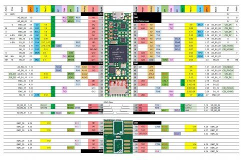
Teensy 4.1 Digital I/O pin map

Status
Not open for further replies.
I've spent a couple of hours now trying to figure out what the "pre-defined" names of the digital I/O ports are.

In the Arduino, the ports are assigned letters, like PortA, PortB, PortC, PortD.

On this page, there is a nice table that shows which pins are assigned which port letters, but it is for the T2.0.
https://www.pjrc.com/teensy/td_digital.html

Is there such a table for the T4.1??? Does anyone know where I can find documentation for what the digital I/O pin assignments are?

Thanks!
 
Thanks!

I'm sure these links will provide a lot of the information I need.

But maybe I'm going in the wrong direction. I have written some C programs for a standard Arduino that uses one of the 8-bit ports, and I'm hoping that I can just load them into the T4.1 and run it without modification (at first). But, I don't know how the pins on the 4.1 map to an Arduino. So that's what I'm actually looking for.
 
Does anyone know where I can find documentation for what the digital I/O pin assignments are?

The pins to native port name mapping is documented on the schematic.

https://www.pjrc.com/teensy/schematic.html

The port names to GPIO register mapping is documented in the reference manual

https://www.pjrc.com/teensy/datasheets.html

Look on page 304-307 for the mapping info. On those pages you'll see the ports as GPIO1 to GPIO4.

Each port has 2 copies, a fast version and a DMA-accessible version. On Teensy you would normally access the pins on GPIO6 to GPIO9, which are the fast ones. So when you see the documentation say GPIO2, plan on actually using GPIO7.

The actual GPIO registers are documented in chapter 12. The registers are listed on page 962.


I have written some C programs for a standard Arduino that uses one of the 8-bit ports, and I'm hoping that I can just load them into the T4.1 and run it without modification (at first).

I'm afraid that just will not work. If you look on page 961, you'll see this:

There are eight 32-bit GPIO registers. ... Only 32-bit access is supported.

There are actually 9, not 8 (which is typical... NXP's documentation is riddled with these sorts of minor errors).

But the really important detail which is true is the GPIO registers do not support 8 bit access. You can't do any 8 bit access and expect to write to just those 8 bit and leave the other 24 untouched. The 32 bit GPIO registers in Teensy 3.x do support that sort of 8 bit access, but on Teensy 4.x the GPIO registers are strictly 32 bits.
 
The Teensyduino documentation on this page doesn't mention this. Is there another link for info on how to use Teensyduino for the 4.1?
https://www.pjrc.com/teensy/td_digital.html

To write the 8-bits (the variable "Phases" in my program) to port D in the Arduio code, I simply used this:

// Output the data to Port D
PORTD = Phases;

The documentation I reference above seems to say that this is the way to do it in Teensyduino.

So for the Teensy 4.1 I would use:
GPIO9 = Phases; // Where "Phases" is a 32-bit number
 
Last edited:
OK, after examining the schematic https://www.pjrc.com/teensy/schematic.html
and the table on pages 304-307 of the manual https://www.pjrc.com/teensy/IMXRT1060RM_rev2.pdf
It looks like the designers of this board connected parts of each port to the edge pins, and parts of the ports to other devices like the memory or whatever.
Maybe GPIO port 1 will work. It looks like bits 16-29 might be available. But, writing a 32-bit word to Port 1 might seriously mess up whatever else bits 0 - 15 are connected to.
There are applications where you need to change a number of bits in parallel simultaneously, not one at a time.
Since this is what I need to do, if there aren't 8 consecutive bits from any one port available to the outside world that I can write to in parallel, the Teensy 4.1 is useless for my application, or anyone's application where they need to output (or input) a byte at a time.
 
Last edited:
OK, after examining the schematic https://www.pjrc.com/teensy/schematic.html
and the table on pages 304-307 of the manual https://www.pjrc.com/teensy/IMXRT1060RM_rev2.pdf
It looks like the designers of this board connected parts of each port to the edge pins, and parts of the ports to other devices like the memory or whatever.
So, writing a 32-bit word to a port would seriously mess things up.
There are applications where you need to change a number of bits in parallel simultaneously, not one at a time.
Since this is what I need to do, it looks like the Teensy 4.1 is useless for my application, or anyone's application where they need to output (or input) a byte at a time.

see first link in post #2 for T_4.1 - it has collected those bits and there are no less than 8 pins sequentially - though not in order on edge pins.
 
I see that most of Port 1 is available. I saw that and corrected my post before seeing your response.

I don't need to have consecutive bits, nor do I need them in order.

The question now is how to set up the port and write to it. The documentation for programming from PJRC.com is sparse.

Hopefully I can find an example of a program where someone has done this.

I'm trying to use this for a school project and the end of the term is quickly approaching. I've been working on this for weeks now, and I'm getting panicky. I'm creating a multi-phase inverter and to control the switches with the proper timing, I need to be able to change the state of all 6 or 8 gate drivers simultaneously. Clocking the data into a shift register would slow things down even more. I have to do some calculations to determine the PWM on/off time to follow the reference fundamental sinusoids at a switching frequency in the 10s of kHz. The Arduino isn't fast enough. The output timing of a Raspberry Pi isn't consistent because it runs Linux, so I was hoping that I could just use the software I already created for my Arduino on a much faster processor. The end goal is to study ways to reduce the noise created by the power transistor switching, so I need to make the hardware perform as close to the "ideal" MATLAB simulations as I can make it.
 
Last edited:
There are examples 'posted' in bits and pieces around.

The most recent is the OV Camera reading 8 bits of camera data two bytes per pixel for a full VGA screen

Though indeed as noted selective read and write is needed to isolate the desired bits and not affect the others
 
You'd need an emulation layer for that, I think a better approach is translate the code from direct port access
back to digitalRead/digitalWrite calls, so its portable, then that should work on the T4. The T4 is about 100 times
faster so you probably will meet any timing requirements - especially if you disable interrupts during the bunches
of updates.
 
re:
Code:
to digitalRead/digitalWrite calls, so its portable

Not portable but this is FASTer/fastest on Teensy with const pin #'s:
Code:
digitalReadFast() / digitalWriteFast()
 
If the pins are in a single port you can do a read/modify/write update operation to the ouput data register to change only the bits/pins you are interested in a single write operation.
 
Warning Read/Modify/Write - can be very unsafe depending on what else is going on. That is I have spent time in the past where I would do something like that, but then maybe running some
Servo update code that a timer interrupt happens and the underlying code changes the state of a servo pin, which may be one of your unused pins. And suppose that ISR happens just after your code did the read of the register. Your modify/write part of the code will overwrite whatever that ISR did... Obviously you can disable interrupts around it.

There are some other ways that may not be as atomic, but can get around that issue of touching other pins. That is you don't use the DR register for this. Instead if you can compute which bits you wish to turn on or turn off or toggle and split this up into 1 or 2 or 3 writes you can use the DR_SET, DR_CLEAR and/or DR_TOGGLE registers, Which take a bitmask where a 1 in a bit will change that bit in DR depending on which register you are using, and other bits are left alone.

As was mentioned in earlier posts, I have excel document for T4.x which tries to show different details about the GPIO pins. For example this is an excerpt from the T4.1 part:
T4.1-Cardlike.jpg
Or simple cut and paste from page showing pins in GPIO pin order:
Code:
Pin	Name	GPIO
 1	AD_B0_02	1.02
 0	AD_B0_03	1.03
24/A10	AD_B0_12	1.12
25/A11	AD_B0_13	1.13
19/A5	AD_B1_00	1.16
18/A4	AD_B1_01	1.17
14/A0	AD_B1_02	1.18
15/A1	AD_B1_03	1.19
40/A16	AD_B1_04 	1.20
41/A17	AD_B1_05 	1.21
17/A3	AD_B1_06	1.22
16/A2	AD_B1_07	1.23
22/A8	AD_B1_08	1.24
23/A9	AD_B1_09	1.25
20/A6	AD_B1_10	1.26
21/A7	AD_B1_11	1.27
38/A14	AD_B1_12 	1.28
39/A5	AD_B1_13 	1.29
26/A12	AD_B1_14	1.30
27/A13	AD_B1_15	1.31
10	B0_00	2.00
12	B0_01	2.01
11	B0_02	2.02
13	B0_03	2.03
6	B0_10	2.10
 9	B0_11	2.11
32	B0_12	2.12
8	B1_00	2.16
7	B1_01	2.17
36	B1_02    	2.18
37	B1_03    	2.19
35	B1_12    	2.28
34	B1_13    	2.29
45	SD_B0_00	3.12
44	SD_B0_01	3.13
43	SD_B0_02	3.14
42	SD_B0_03	3.15
47	SD_B0_04	3.16
46	SD_B0_05	3.17
28	EMC_32	3.18
31	EMC_36	3.22
30	EMC_37	3.23
 2	EMC_04	4.04
 3	EMC_05	4.05
 4	EMC_06	4.06
33	EMC_07	4.07
5	EMC_08	4.08
51	EMC_22	4.22
48	EMC_24	4.24
53	EMC_25	4.25
52	EMC_26	4.26
49	EMC_27	4.27
50	EMC_28	4.28
54	EMC_29	4.29
29	EMC_31	4.31
---	----	----
Which is Teensy Pin, The IMXRT pin name, and the GPIO Port.pin
 
Status
Not open for further replies.
Back
Top