
I am working on a project using the teensy 4.1 board where I also use a level shifter to shift it's voltage from 3.3 V to 5V to give it to a DAC. Every time I try to connect the DAC, the USB side of teensy 4.1 (specifically, the voltage and current limiting circuit) starts heating up and I see that the current reading goes to 0.45 A (It usually shows 0.09 to 0.18 A). I am supplying 15 V and -15 V for the DAC to operate and 5V to the microcontroller. I do not understand why this is happening and any help would be highly appreciated.
teensy 4.1 voltage and current limiters heating up
- Thread starter Lalita
- Start date
kd5rxt-mark
Well-known member
I am working on a project using the teensy 4.1 board where I also use a level shifter to shift it's voltage from 3.3 V to 5V to give it to a DAC. Every time I try to connect the DAC, the USB side of teensy 4.1 (specifically, the voltage and current limiting circuit) starts heating up and I see that the current reading goes to 0.45 A (It usually shows 0.09 to 0.18 A). I am supplying 15 V and -15 V for the DAC to operate and 5V to the microcontroller. I do not understand why this is happening and any help would be highly appreciated.
Can you post pictures of your actual wiring (with a good angle of view & sufficient resolution to follow the individual wires) ?? Without that, the only thing we could do would be to make random guesses.
Mark J Culross
KD5RXT
Sorry about the picture in advance, there are no explicit wire connections that can be shown since we are utilising a PCB, and as for the PCB we weren't provided with a layout.
The 5 V and GND from power supply on the PCB goes to the micro-controller. the 15 V and the -15 V go via a connecting cable to another PCB where the DAC is mounted. The level shifter also heats up when the teensy heats up.

The 5 V and GND from power supply on the PCB goes to the micro-controller. the 15 V and the -15 V go via a connecting cable to another PCB where the DAC is mounted. The level shifter also heats up when the teensy heats up.
PaulStoffregen
Well-known member
Even with the PCB schematic and/or layout (are 2 PCBs in play?), and part numbers for the DAC, level shifter, and other parts... this would still be quite a feat to remotely (no hardware in hand to test) troubleshoot over the internet.
Some questions on the diagram...
I see a block called "Level Shifter", with 3 power wires and 3 signals from Teensy. But it lacks output signals. Also has no connection to GND. I'm guessing the actual connections are more involved that we get to see in this diagram?
You mentioned the DAC is on another PCB which is connected by a cable. In the diagram I can see 3 power wires, and 3 pins called "SPI Pins" which don't seem to connect to anything. I can't see any indication of connectors or a cable.
Most DAC chips require at least a decoupling capacitor. Some take other parts. Nothing extra is shown in the diagram.
Still just wondering what the DAC part number is, and which level shifter is used. Can't see any part numbers.
But without this info of the hardware you're connecting, I can at least guess about the heating issue. It's very likely coming from U4, the 3.3V regulator.
Two large vias on the sides of U4 allow its heat to travel into the ground plane inside the PCB, so when U4 dissipates head that entire area of the board tends to become hot. It can be difficult without thermal camera to tell exactly which part is generating the heat, but U4 is the most likely.
If it really is U4, that's a strong sign something is drawing a lot of extra current from the 3.3V power line. From your diagram, sounds like the DAC doesn't even get a connection to 3.3V power. Very difficult to imagine how this is happening, based only on the info shown. By guess is the actual hardware is more complex than we can see...
Here is a better circuit diagram of our connections.
The level shifter TXU0304 gets the 3.3 V and 5 V from the Teensy 4.1 microcontroller. There are a total of 13 such level shifters which are then connected to the DAC. The PCB with the DAC (PCB 2) and the PCB with level shifters and microcontroller (PCB 1) are connectefd to each other via a cable with pin description of X1 in the diagram.
PCB 1 has -15 V, GND, 15 V, GND and 5V pins to provide the respective inputs and has bypass capacitors for all power supply rails. I am currently using a USB from PC to power the teensy.
Teensy's component U4 is heating up sometimes and is causing the teensy to fail. Upon checking with a multimeter, I saw that the teensy's LDO (U4) somehow appears short(Meaning: component failure). We tried to remove it from the teensy and the short disappeared. But that does not fix anything or explain why this keeps happening to us. Some posts in the forum suggested that this can be fixed by using shottky diode between the 3.3 V and 5 V of the teensy. How can this be implemented ? Even after checking my connections multiple times, I can't figure out how my teensy pins are getting a voltage more than 3.3 V causing this failure. There might be a high current path that is causing teensy to fail but I am not sure.
Am I missing any important design consideration here ?
PaulS
Well-known member
1. You don't need a level-shifter if you connect the DAC's Vio pin to 3V3. See datasheet, page 21. All digital signals will be on 3V3 level so can connect to the Teensy directly.
2. Just checking: you are connecting the 5V from the powersupply to the Vin pin of the Teensy?
3. Is it possible to share a complete schematic including Teensy, DAC and powersupply?
4. I don't understand "13 such level shifters", why 13?
Paul
2. Just checking: you are connecting the 5V from the powersupply to the Vin pin of the Teensy?
3. Is it possible to share a complete schematic including Teensy, DAC and powersupply?
4. I don't understand "13 such level shifters", why 13?
Paul
Thank you for that information. I just checked the data sheet and we totally missed that one out earlier.
2. Just checking: you are connecting the 5V from the power supply to the Vin pin of the Teensy?
Yes. Vin is connected to 5 V in our design. But we chose USB to power the Teensy.
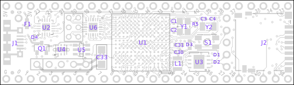
Here is a detailed image.
In addition to what is not included in this image, each level shifter is attached a 100nF capacitor between it's 3.3V and GND pin and 5 V and GND pin seperately.
Again, PCB1 and PCB2 are connected using X1. There are 12 more PCBs connected to PCB1 similarly. We are using this setup to access multiple control elements connected to the different channels of the DAC.


Now, we are using 13 level shifters because we wish to control 13 peripherals (same CLK and MOSI, different CS for each slave) with the microcontroller. Each peripheral has its own DAC and MUX. Therefore, using the level shifters, the idea was to level shift the logic to 5 V and provide the DACs. MUX is just to get a feedback and read it at the controller but that is not yet connected to anything. It is supposed to be an addition for the future.
Do you think that adding thislevel shifter in between is casuing issues with our system, because there is some path that us giving us a high current and everything connected between 3.3 V and GND are going dead (all level shifters and Teensy) as a result of that (most likely) current. Also, this happens mostly when we connect the second PCB (DAC and MUX) to the first PCB (Teensy and level shifters).
2. Just checking: you are connecting the 5V from the power supply to the Vin pin of the Teensy?
Yes. Vin is connected to 5 V in our design. But we chose USB to power the Teensy.
Here is a detailed image.
In addition to what is not included in this image, each level shifter is attached a 100nF capacitor between it's 3.3V and GND pin and 5 V and GND pin seperately.
Again, PCB1 and PCB2 are connected using X1. There are 12 more PCBs connected to PCB1 similarly. We are using this setup to access multiple control elements connected to the different channels of the DAC.
Now, we are using 13 level shifters because we wish to control 13 peripherals (same CLK and MOSI, different CS for each slave) with the microcontroller. Each peripheral has its own DAC and MUX. Therefore, using the level shifters, the idea was to level shift the logic to 5 V and provide the DACs. MUX is just to get a feedback and read it at the controller but that is not yet connected to anything. It is supposed to be an addition for the future.
Do you think that adding thislevel shifter in between is casuing issues with our system, because there is some path that us giving us a high current and everything connected between 3.3 V and GND are going dead (all level shifters and Teensy) as a result of that (most likely) current. Also, this happens mostly when we connect the second PCB (DAC and MUX) to the first PCB (Teensy and level shifters).
Attachments

PaulS
Well-known member
Just to recap to make sure I understand:Do you think that adding thislevel shifter in between is casuing issues with our system, because there is some path that us giving us a high current and everything connected between 3.3 V and GND are going dead (all level shifters and Teensy) as a result of that (most likely) current. Also, this happens mostly when we connect the second PCB (DAC and MUX) to the first PCB (Teensy and level shifters).
- PCB1 contains a Teensy 4.1, 13pcs TXU0304 and 13pcs X1 connector.
- PCB2 contains one DAC and one analog mux.
- The system will consist of one PCB1 and 1-13pcs PCB2's.
Currently, are all Vcca pins of the 13 levelshifters connected to Teensy pin 3V3? And are all Vccb pins of the 13 levelshifters connected to an external 5V powersupply?
Is PCB1 is running fine without any PCB2 connected?
If one or more PCB2's are connected, PCB1 fails with U4 overheating and Teensy not running?
About powering over USB: if you power the Teensy over USB, the USB voltage will be present on the Teensy Vin pin. That same Vin pin is also connected to the external 5V powersupply. That is not good.
My suggestion would be to cut the external 5V power supply from the Teensy Vin pin. And insert a regular 1N4001 diode from the external 5V power supply to the Teensy Vin pin.
That way the USB 5V will never power the external circuitry. And if you run the Teensy without USB, the Teensy will be powered by the external 5V through that diode.
Paul
Yes. All Vcca pins of the 13 level shifters are connected to Teensy pin 3.3 V, and all Vccb pins of the 13 level shifters are connected to an external 5V power supply.(This is also connected to Vin pin as you know).
PCB1 normally runs fine but suddenly, we see U4 and level shifters heating up after a while.
We never came so far to connect PCB2 alongside PCB1.
PCB1 normally runs fine but suddenly, we see U4 and level shifters heating up after a while.
We never came so far to connect PCB2 alongside PCB1.
PaulS
Well-known member
Since there are only level shifters connected to the Teensy 3V3 pin, we need to focus on that part now.
Can you measure the resistance from the 3V3 to GND at an unpowered PCB1?
Is it possible to disconnect the Teensy 3V3 pin from the rest of te circuit (perhaps by cutting a pin or trace)? We need to check whether the Teensy runs fine without an external 3V3 load.
An idle sitting TXU0304 levelshifter should use very little current.
With respect to signals SDI and SDO: SDO is an output of the levelshifter and thus inputted to the Teensy (and SDI is an input of the levelshifter and thus an output of the Teensy). Can you check whether that configuration is indeed as intended (and your Teensy software is setup such as well)?
Paul
With respect to signals SDI and SDO: SDO is an output of the levelshifter and thus inputted to the Teensy (and SDI is an input of the levelshifter and thus an output of the Teensy). Can you check whether that configuration is indeed as intended (and your Teensy software is setup such as well)?
Just a small clarification here, we initially had this connection as shown in the image, but later, interchanged the SDI and SDO pins which go to the low side of the level shifters. Also, OE is connected to 3.3V.
If all the SDO outputs from the level shifters are connected together and their OE is connected to constant 5V, they're all driving that line at the same time - shorting 3.3V to GND if one tries to output HIGH and another outputs LOW at the same time.
Can you please elaborate this please ?
Intead of having all the level shifters soldered on the PCB, we are having only one level shifter to make sure that we don't lose too many components when this burn out happens (which is quite freqent).
Can you measure the resistance from the 3V3 to GND at an unpowered PCB1?
170 Ohms. Is it possible that upon performing a continuity test, there might appear a short between CS pin and GND pin of the level shifter but it does not necessarily mean that the level shifter is probably burnt. ?
Is it possible to disconnect the Teensy 3V3 pin from the rest of the circuit (perhaps by cutting a pin or trace)? We need to check whether the Teensy runs fine without an external 3V3 load.
An idle sitting TXU0304 levelshifter should use very little current.
I will need some more time to get back to you with these results.
Just explaining the order of things again:
There is something that is happening at the level shifter's end when we connect the DAC and MUX boards (PCB 2) to PCB 1. Whenever this current spike occurs,the level shifters start to heat up and I notice a short between 3.3 V and GND of level shifter as a result of the chip failing. This being connected to teensy, if I am not quick enough to disconnect teensy from the rest of the circuit is causing the LDo on teensy as well to heat up and burn the teensy.
There is something that is happening at the level shifter's end when we connect the DAC and MUX boards (PCB 2) to PCB 1. Whenever this current spike occurs,the level shifters start to heat up and I notice a short between 3.3 V and GND of level shifter as a result of the chip failing. This being connected to teensy, if I am not quick enough to disconnect teensy from the rest of the circuit is causing the LDo on teensy as well to heat up and burn the teensy.
Just a small clarification here, we initially had this connection as shown in the image, but later, interchanged the SDI and SDO pins which go to the low side of the level shifters. Also, OE is connected to 3.3V.
This is not clear. Are the connections as shown in your image, or are they not? How can we help you if we're not shown the correct information?
We need full details of how all chips in the project are connected, not just one diagram and a statement that there are multiple instances of it.
It sounds like you have multiple SDO outputs from the level shifters tied together, connecting to the single SDO pin on the Teensy. That is simply not going to work because all of the level shifters will be trying to drive that signal at the same time.
I also don't see the need for multiple level shifters all translating the same SDI/SCK/SDO signals - you could just tie them together on the 5V side, put them through a single level shifter and connect them to the Teensy. That would automatically solve the SDO contention issue since only one DAC would drive it at a time (when CS is high it is high impedance).
BriComp
Well-known member
Intead of having all the level shifters soldered on the PCB, we are having only one level shifter to make sure that we don't lose too many components when this burn out happens (which is quite freqent).
Can you measure the resistance from the 3V3 to GND at an unpowered PCB1?
170 Ohms. Is it possible that upon performing a continuity test, there might appear a short between CS pin and GND pin of the level shifter but it does not necessarily mean that the level shifter is probably burnt. ?
Is it possible to disconnect the Teensy 3V3 pin from the rest of the circuit (perhaps by cutting a pin or trace)? We need to check whether the Teensy runs fine without an external 3V3 load.
An idle sitting TXU0304 levelshifter should use very little current.
I will need some more time to get back to you with these results.
Can you put the bits of text that you are answering into /QUOTE tags.
That way we know what is the oroginal question and what is the answer.
By way of an example below is the configuration of your post above with this applied.
170 Ohms. Is it possible that upon performing a continuity test, there might appear a short between CS pin and GND pin of the level shifter but it does not necessarily mean that the level shifter is probably burnt. ?Intead of having all the level shifters soldered on the PCB, we are having only one level shifter to make sure that we don't lose too many components when this burn out happens (which is quite freqent).
Can you measure the resistance from the 3V3 to GND at an unpowered PCB1?
I will need some more time to get back to you with these results.Is it possible to disconnect the Teensy 3V3 pin from the rest of the circuit (perhaps by cutting a pin or trace)? We need to check whether the Teensy runs fine without an external 3V3 load.
An idle sitting TXU0304 levelshifter should use very little current.
Okay, I will try to summarize all the answers I gave before into a single post here.
Just a small clarification here, we initially had this connection as shown in the image, but later, interchanged the SDI and SDO pins which go to the low side of the level shifters.
This means, the SDI and SDO pins of all the level shifters are just interchanged on Vcc A side recently. Pin 4 on Vcc A is SDO and pin 5 on Vcc A is SDI.
Also, OE of all level shifters is connected to 3.3V. The guy who designs the PCB did it that way.
I am sorry for not giving this information earlier. I don't have this update in the schematics yet. This is something we changed quite recently after carefully examining the board. So these are the only 2 deviations from the original schematic images I shared with you, but rest is all the same.
Instead of having all the level shifters soldered on the PCB, we are having only one level shifter soldered to the board at a time to make sure that we don't lose too many components when this burn out happens (which is quite frequent). But the original design that we are working on is exactly the same as explained before, with 13 level shifters.
170 Ohms.
Now, my question here is:
Is it possible that upon performing a continuity test, there might appear a short between CS pin and GND pin of the level shifter but it does not necessarily mean that the level shifter is probably burnt. ?
I am trying to give out as much info as possible here. Please let me know if you need any more details from my end.
With respect to signals SDI and SDO: SDO is an output of the levelshifter and thus inputted to the Teensy (and SDI is an input of the levelshifter and thus an output of the Teensy). Can you check whether that configuration is indeed as intended (and your Teensy software is setup such as well)
Just a small clarification here, we initially had this connection as shown in the image, but later, interchanged the SDI and SDO pins which go to the low side of the level shifters.
This means, the SDI and SDO pins of all the level shifters are just interchanged on Vcc A side recently. Pin 4 on Vcc A is SDO and pin 5 on Vcc A is SDI.
Also, OE of all level shifters is connected to 3.3V. The guy who designs the PCB did it that way.
I am sorry for not giving this information earlier. I don't have this update in the schematics yet. This is something we changed quite recently after carefully examining the board. So these are the only 2 deviations from the original schematic images I shared with you, but rest is all the same.
Instead of having all the level shifters soldered on the PCB, we are having only one level shifter soldered to the board at a time to make sure that we don't lose too many components when this burn out happens (which is quite frequent). But the original design that we are working on is exactly the same as explained before, with 13 level shifters.
Can you measure the resistance from the 3V3 to GND at an unpowered PCB1?
170 Ohms.
Now, my question here is:
Is it possible that upon performing a continuity test, there might appear a short between CS pin and GND pin of the level shifter but it does not necessarily mean that the level shifter is probably burnt. ?
I am trying to give out as much info as possible here. Please let me know if you need any more details from my end.
Instead of having all the level shifters soldered on the PCB, we are having only one level shifter soldered to the board at a time to make sure that we don't lose too many components when this burn out happens (which is quite frequent). But the original design that we are working on is exactly the same as explained before, with 13 level shifters.
Then you're going to have to change it, because it's not going to work; you can't tie the outputs from the A side of the level shifters together (the signal that connects to pin 12 on the Teensy) without any extra gates. A logic signal should only be driven by a single device at any point in time, and all the level shifters have their outputs permanently enabled by tying their OE pin to a HIGH level. Regardless of it being the cause of your current problem, you might as well address it first because it's going to be a show-stopper.
Good observation! Yes, combining all the SDO signals is not going to work this way.
Wonder if the OP needs to be able to read the DAC(s). If not, get rid of all the SDO signals.
Paul
If we were to actually need these SDO signals, how should we implement this on the PCB ? I still am confused about this because, conceptually, we use Slave Select to read something from a particular peripheral or write something to it. why should it be a problem for us? Sorry, if this is a very basic question

I'll try and explain it a bit better.
So you've got all the SDO signals coming out of the DACs, all going in to one input on the Teensy. According to the DAC datasheet, the SDO pin is only driven when the corresponding CS pin (what you just referred to as Slave Select) is active - so only one device should be driving the input on the Teensy at a time, right? Wrong. Because you've got those level shifters in the way - they don't sense when their inputs aren't driven, they always output something (either a high or a low) unless their OE pin is inactive - which in your case never happens because they're tied high. So you end up with a case where one level shifter will be outputting low (connecting the line to GND) and another will be outputting high (connecting the line to 3.3V). That's effectively shorting 3.3V to GND via the level shifter ICs.
What you could do is control the OE pin on each level shifter at the same time as CS for each DAC, but from the looks of the circuit they are different polarities (CS is active low, OE is active high).
Have you looked into the idea mentioned earlier in this thread of using 3.3V for the DAC's VIO pin? That would apparently eliminate the need for the level shifters and solve the problem.
Last edited: