24 bit audio boards

About the pin 10, you are right. I would also connect pin 9 directly to the capacitor pad
The 5V was a misunderstanding from my side, I just gave the datsheet a quick glance. Thought that you were making 1.8 from 3.3 V. Now that I read it again, only the digital part is capable of 1.8V.

As for the decoupling, there are now 2x 10uF on the same line. uF capacitors are only for the low frequencies, where it does not matter where you place it on the line.
The input of the regulator only has a 2.2uF capacitor, which again is only for low ferquencies. To keep out the higher frequencies, place eg a 10nF at the input, to clean up the voltage, before it goes into the regulator. This will help the regulator generating a clean voltage.

For the diode, just a thought, does anything happen when you feed back 5V to the main connector? Maybe use a diode from the main connector as well?
As for the decoupling of the J1, this was for 800 MHz and higher. You placed it after the diode, so detection will already have happened. You would want to place it before the diode. Also because of the frequency, give it two vias directly to ground near the pad, and route the trace so that the current goes over the capacitor. Now the return current has to take a detour of about 12mm before it reaches the groundplane, just being lazy and assuming 1nH/mm (it will be worse), it will have 12 nH of induction. At 800 MHz, the impedance will be 60j ohms, so hardly any decoupling.

Now that I think about it do the same to the L/R output. Add a second via to the round and connect the lines to the pad of the capacitor, so that all signal travels over the capacitor first.

Finally the ground plane of the charge pump. You can explain this in two ways:
1: the pump frequency will be outside of the audible frequencies, so for the rest of the spectrum it can be assumed clean. The digital ground plane can be assumed dirty for all spectral components, so it should be kept far away from the analog ground so the ground plane is OK.
2: The pump signal will be huge and the digital spurious is assumed to be small, therefore you would want to contain the pumping signal as much as possible, so make this ground plane as small as possible and route the digital ground around it.
I do not know which is better.
 
kpc,

You rock! I am sure I did not comprehend all of it, but definitely have a little bit better understanding of this complex process. Also, thanks to the forum for bearing with me here. I will use this thread and my board layouts as I go along when I have to do something like this again.

The final is attached. I'll be ordering boards in the next few days for my raspberries. If anyone wants the eagle flies to use as a basis for a teensy 3.1 based version of one of these DACs , let me know.

Keith
 

Attachments

  • ver_4.zip
    20.9 KB · Views: 314
Some final comments: the vias should be placed next to each other, to reduce inductance, not after each other. The way you placed them will give roughly 10% reduction of induction compared to a single via. If you place them next to each other, you get approximately 30% reduction. If you place them on opposing sides of the pad you get 50% reduction in inductance. Like the third one in this picture. The last option in the image is worse, assuming you chose a standard thickness of 1.6 mm (1/16"). The final one will only be better when using a multi-layer board with thin layers (< 0.4mm), also there are some manufactering issues associated, like tombstoning and capilary suction of the solder (sorry do not know the proper english term). The latter could be prevented using plugged vias (at a cost).
Another final touch would be to route the trace at J1 from the connector to the capacitor and then continue from the capacitor pad.

I am really curious about the actual performance of this device. I hope to see some measurements results.
I do not know if you know someone with a decent spectrum analyzer, to examine the output spectrum. If not, an alternative way is to output two 1 kHz sine waves. One at each L/R output, but with opposite phases. Then use two resistors to add the sines. This allows to somewhat examine the spurious on the output with an oscilloscope. Ideally the output should be zero (after aligning the gains). What remains is the effects of power supply ripple, as well as all even order harmonics. The odd order harmonics will unfortunately be cancelled this way.
 
kpc,

I changed the pads to be like the example 3. I did not make that 'final touch' change, though, as I forgot before I sent it off. I'll not be using the external 5V, though. We have a sophisticated scope here at work but no dedicated spectrum analyzer. After I get the boards back and populated, Maybe you can help guide me through how to test this. Are there test files in *.wav or other digital format that I can play through this? Like I said, the eagle files are available to whomever may want them (for non-commercial use).

Keith
 
Yes, I could help. As for the audio, if you have octave (free) or matlab, you can generate the sines this way:
Code:
t = 0:(1/44100):10;
v(:,1) = sin(2 *pi * 1e3 * t);
v(:,2) = -sin(2 *pi * 1e3 * t);
wavwrite(v, 44100, 16, 'out.wav');
You would want to generate this file yourself, to compensate for gain differences between left and right, to achieve good cancellation of the fundamental.
 
An update at last!

I finally got the rest of the board assembled and was able to do some preliminary testing this evening.

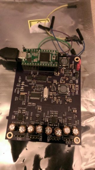
Here's picture of the completed board along with my 'loopback cables' :) (taken with my terrible cell phone camera):
IMAG1227.jpg

I have some quick test results as well:

Edit: All the plots are for a sample rate of 48kHz.
Edit2: There is no A-weighting on any of these plots (or the THD+N calculation).

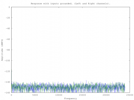
Input noise with inputs grounded (4096 pt capture, no averaging):
test3_resp.png

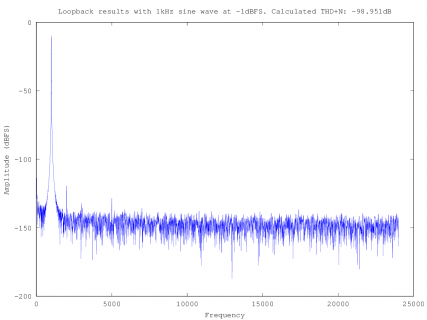
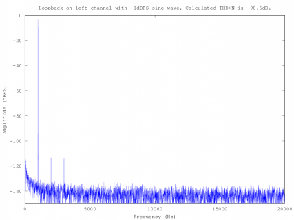
Loopback with -1dBFS sine wave at 1KHz (8192 pt capture, no averaging, left channel only):
loopback_results_THD_N.png

I'm pretty happy with the performance. There aren't any spurious signals sticking up anywhere (even with my cheap loopback setup), and the performance is pretty darn close to the CS4272 specs, as designed.

I'll do some more testing tomorrow, but everything is looking good so far!
 
Last edited:
@whollender. Looks pretty good.
Since you apply loopback, the ADC and DAC are syncronized, therefore you can choose a 'nice' frequency, so that you can remove the windowing and look also close-in to the carrier. "Nice" frequencies are a multiple of AUDIO_SAMPLE_RATE_EXACT/N_FFT, so 2.69 Hz, so a good 1 kHz candidate will be round(1000/df)*df = 999.002 Hz.

I also notice that you have the carrier at -8dBFS, did you already tweak this for the highest possible dynamic range? Usually ADC's are measured at -1dBFS, although I agree for audio applications a lower value is more representing the typical use.

Edit: one minor thing with loopback is that it does not show spurious effects on the reference voltage.
Edit2: Just noticed that the heading says it was at -1dBFS, so maybe the results were not corrected for windowing loss?
 
Last edited:
@kpc, I did screw up the scaling (I was up too late and trying to get the plots off before my laptop battery died). The whole plot should be ~6dB higher (forgot to scale for max sin amplitude of -3dB and also grabbed the positive half spectrum without adding in the negative side for another 3dB). I did compensate for window loss.

Another reason why the results are lower is that the output impedance of the DAC buffers isn't really low (~100), and the input impedance of the ADC buffers isn't particularly high (~1k), so another ~dB of loss.

I don't have it working with the audio library at the moment (I've been doing everything bare metal), so I just used 1kHz exactly because the sample rate is an exact multiple of it, so I could just use 48 coefficients and not have to worry about interpolation. I can do something similar to the exact sample rate with a DFT length that isn't a power of 2. Octave uses FFTW, which is supposed to handle odd length ffts just fine.

I'm planning on doing some more testing for things like SNR (with -60dBFS sine wave), performance with single-ended inputs and outputs, crosstalk, frequency response, higher sampling rates, etc. , so I'll have plenty more to look at.
 
Last edited:
Ready to share the PCB? I'd love to get a bare PCB and build one here.

Don't know when I'll manage to get into the I2S code again.... but this ought to give me some incentive!
 
Ready to share the PCB? I'd love to get a bare PCB and build one here.

Don't know when I'll manage to get into the I2S code again.... but this ought to give me some incentive!

I need to make a few tweaks to the silkscreen and decide what license to use (I'm still deciding whether to try selling populated boards, which may have an impact on how I share the design files), but I should have it up soon.
 
@whollender, about the audio library, forgot that it only supports 16 bit (for now).
About the fftw/octave, never had problems with it. Even for prime number of points, the FFT still outperforms a normal DFT. So just use an integer multiple of 48 for the FFT and you can remove the window.
Since you use octave, to improve your images, you could integrate (average) multiple spectra in the voltage domain, to assess harmonics. This should lower your noise floor by sqrt(N), where N is the number of averages.
To assess the noise floor itself, you can integrate multiple spectra in the power domain. This will reduce the standard deviation of the noise floor by sqrt(N).
If you want to search for spurious from the power supply, perform integration in the power domain, because the switching will not be synchronized to the sampling.


If you would not mind, I would be very interested in three further measurements.

The first one is isolation. I assume you would already be performing this one yourself. Put a sine on the left DAC out and zeros n the right DAC out. Then measure the signal coming in the right ADC.

The second is the noise level with the either inputs open circuited, or loaded with a resistor > 1k.

The third one is more related to my personal interest (ie not audio) and I can imagine you are not interested in performing this test (would not blame you).
This test would be a two tone test to assess the second and third order intermodulation products (IM2/IM3) or 2nd and 3d order intercept points (IP2/IP3). Two tones at say 5 and 6 kHz, each tone at -7 dBFS (ie worst peak at -1dBFS)
The code below gives you the samples. I kept it at the same 48 samples as your 1 kHz tone.
Code:
fsample = 48e3;
f1 = 5e3;
f2 = 6e3;
fg = gcd(f1,f2);
t = 0:(1/fsample):(1/fg - 1/fsample);
v = 0.5 * sin(2*pi*f1*t) + 0.5 * sin(2*pi*f2*t);
v *= 10^(-1/20); % -1dBFS
v = round(v * 2^23); % scale to 23 bit
 
kpc,

I had planned on playing around with some averaging to do some spur hunting. I can do synchronous voltage domain averaging on the teensy pretty easily by just summing into a circular buffer (works as long as the buffer length is an integer multiple of the signal period). I might be able to do something similar in the power domain, but I'd probably have to double the bit depth in the buffer so that I can square the signal without loss of fidelity.

I was definitely planning on doing an isolation measurement (I called it crosstalk in my previous post, which isn't really the right term for analog). And I actually have some measurements already with open inputs that I'll post later today when I get home.

I hadn't thought of doing any testing of intermods, but that's a pretty good idea. I don't think you see it very often in audio because the relative bandwidths are so high, whereas in RF and up your measurement BW is small enough compared to the fundamental freq that you can't simply measure all the harmonics of the signal.
 
@whollender. This is for an RF application (hobby). I am looking for the doppler shift of a modulated signal of only up to 1 kHz, partly hidden within the bandwidth of the modulation itself. So in this case it is intermods of the reference signal itself. I work(ed) in radar and radio astronomy, but I believe the telecom guys would call this the shoulders of the ACPR. You can easily calculate the shoulders, knowing the IP3 (and the modulation properties).
 
Hey kpc,

That sounds like a pretty interesting application. Here are some more results:

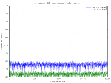
Left channel with open inputs:
Inputs_open_left_ch.png

-1dBFS loopback with synchronous fft:
THD_N_Left_ch.png

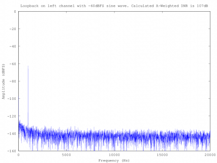
-60dBFS loopback with synchronous fft:
DNR_l.png

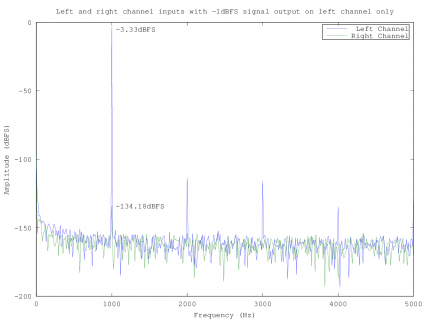
Isolation test (-1dBFS 1kHz sine wave on left channel, measuring left and right channels on input, with 256 averages):
Isolation_left_out_max_avg.png

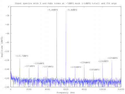
Two tone test (5kHz and 6kHz sine wave with -7dBFS amplitudes each, 256 averages):
Intermods_5_6_kHz_max_avg.png

I added a bunch of averaging to the two tone and isolation tests so that the peaks were clear of the noise floor.

The SNR is a bit lower than I had hoped, but the noise for the input and output are adding, so it should be about 3dB higher individually (assuming the noise amplitudes are the same input vs output). If you add 3dB to the dynamic range, it's about 110dB, which is pretty close to the claimed 114dB on the CS4272 datasheet.

I've been updating the board files to include some better annotation on the silkscreen for the inputs and outputs. I also did one small routing change (moved two resistors to other side of board), so I want to double check the gerbers before I put them up. I should have them on github soon.
 
I have to say, I am impressed with the results.

Just cross-checked the harmonics with the intermods and they seem to be consistent.
Also the 5th and 7th harmonic is pretty dominant, so the cause might not be nonlinearity in the amplifiers/S&H, but in the actual A/D converter itself. Also now by checking the datasheet I see that the THD does not track the input power, which is another indication. Anyway pretty decent results.

As to the dynamic range, the 114 dB in the datasheet is A-weighted. I would suspect you are using unweighted results, so if you compare this to the 111 dB in the datasheet, you are pretty close. As to the 3dB increase, just by eyeballing, this is a reasonable assumption. When I check both the open and short circuited noise floor, then the loopback seems about 3 dB higher, so you are probably not too far off.

Thank you whollender for these measurements.

Edit: Oops, I now see in the heading of the figure, that you used A-weighting.
 
Last edited:
Thanks, kpc.

I finally got around to putting the files up on github, and the project is released on oshpark as well.

Edit: updated oshpark link to the fixed version of the board.

I did make some changes to the board design that is provided which have not been tested, but the changes are very minor. The most major change is that I moved two resistors from the top layer to the bottom layer so that I could fit more silkscreen annotations on the analog IOs. The 0 ohm resistors only shorted the analog input grounds to the board ground, so there isn't much risk there. I also added a lot of annotations to the silkscreen on the analog IOs, and a bit at the power supply input. Finally, I also added some copyright notices, along with the license I'm releasing the files under (Creative Commons CC-BY-SA-NC v4.0).

Next up is a frequency response test, and some testing at higher sample rates.
 
Last edited:
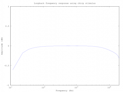
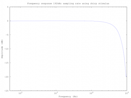
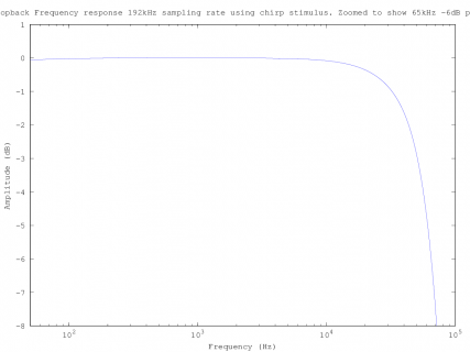
192kHz sample rate works! The mk20 chip doesn't specify it's I2S interface very well, so I wasn't sure if it would work with the isolator ICs slowing the interface down.

Here are a couple of frequency response plots:

@ 48kHz sample rate:
Freq_resp_right_channel.png

@ 192kHz:
Freq_resp_r_ch_192k.png

@ 192kHz zoomed to show -6dB point (-3dB for input and output, assuming same freq response):
Freq_resp_r_ch_192k_zoomed.png
 
along with the license I'm releasing the files under (Creative Commons CC-BY-SA-NC v4.0).

If I order 10 of these boards from iTead, would it be acceptable to offer 8 of them for free, but shipped together with regular Teensy orders? I think that probably counts as "non-commercial", but since it would be piggybacking on the commercial sales of Teensy orders, just want to get a confirmation that would be ok with you?
 
If I order 10 of these boards from iTead, would it be acceptable to offer 8 of them for free, but shipped together with regular Teensy orders? I think that probably counts as "non-commercial", but since it would be piggybacking on the commercial sales of Teensy orders, just want to get a confirmation that would be ok with you?

Paul, I'm completely ok with that. Let me know if you have any issues with the files, or if anything is unclear.
 
Ok, I've ordered 10 pieces from iTead. I imagine they'll get here in a month or so.

When they do arrive, I'll mention it on this thread. I'm not going to make a special announcement. But anyone who's been following this thread and remembers can request one when ordering a Teensy 3.1 from PJRC. Just mention this message in the "additional instructions" box. I'll probably build one, keep one board as a spare, and ship the other 8 (just the bare PCB). Please, since there's only 8, request one only if you're pretty sure you'll actually build it.
 
Thanks, kpc.

I finally got around to putting the files up on github, and the project is released on oshpark as well.

I did make some changes to the board design that is provided which have not been tested, but the changes are very minor. The most major change is that I moved two resistors from the top layer to the bottom layer so that I could fit more silkscreen annotations on the analog IOs. The 0 ohm resistors only shorted the analog input grounds to the board ground, so there isn't much risk there. I also added a lot of annotations to the silkscreen on the analog IOs, and a bit at the power supply input. Finally, I also added some copyright notices, along with the license I'm releasing the files under (Creative Commons CC-BY-SA-NC v4.0).

Next up is a frequency response test, and some testing at higher sample rates.

Just a heads up. You forgot the ":" in the URL for the link at oshpark to this forum thread.
 
@kpc

Update. I got the boards back and soldered one together tonight. It 'works', but there is a huge 60Hz buzz when I touch the ground (USB shield for example).

Did a little checking and I have the pinouts on the rca jacks wrong (gnd and pin reversed). The 3.5mm jack is correctly connected, though, so I can try to test it. I will see if I can get to it tomorrow night and make any reasonable measurements. So, Rev 3 will be what I release on osh park with correctly connected rca jacks...

Keith
 
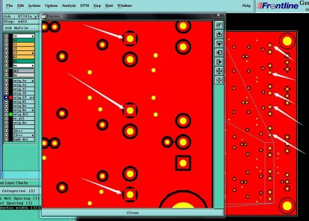
Itead responded with this question:

Your gerber file: SuperAudioBoard.zip (Normalized Name:I00xxxxxAN_A4CGHA002A.zip) in the order #1000xxxxx has an issue:

Please see the picture attachedm, the component holes are connected with the copper layer.
Is that right?

1.jpg

Indeed, it does seem like those square pads have signals routed to them, which short to the internal plane.

Did they work on the OSH Park board?
 
Back
Top